

The printed circuit board (PCB) is the heart of almost any electronic product, carrying the components and copper wires supporting its functionality. The manufacture often involves electroplating, a process that can vary between designs. This leaves you, the engineer behind its simulation and optimization, constantly creating new models. What if you could push much of this work onto the designers, engineers, and technicians behind its design and manufacture, having them run their own electroplating simulations for PCBs? See how here.
Tailored Electroplating Simulation Apps
A tailored electroplating app can be built using the Application Builder and the Electrodeposition Module in COMSOL Multiphysics version 5.0. With this resource, PCB designers can use simulation to analyze a number of factors in the design and manufacturing process. They can evaluate whether a design will be adequate for achieving copper wiring specifications, assess the performance of such devices, and estimate the electroplating process’ manufacturing cost, without any prior knowledge of electroplating.
Design Challenges of the Copper Pattern Plating Process
A common printed circuit board (PCB) uses a layer or multiple layers of copper wires to connect to the board’s active and passive devices. The more advanced PCBs, on the other hand, use copper pattern plating to generate the wires. Before the actual electroplating process can take place, the PCB needs to be prepared with a patterned insulating film. This particular process is done in a number of steps.
Preparing the PCB with a Patterned Insulating Film
The first step is to cover the PCB with a thin conducting copper seed layer. Next, the PCB’s surface needs to be coated with a photoresist (a photosensitive polymer film), a process referred to as photolithography. This process exposes the resist to ultraviolet light through a patterned photomask and then dissolves the areas that were exposed. The result is a PCB with a patterned insulating film that exposes the seed layer on the bottom of the pattern.
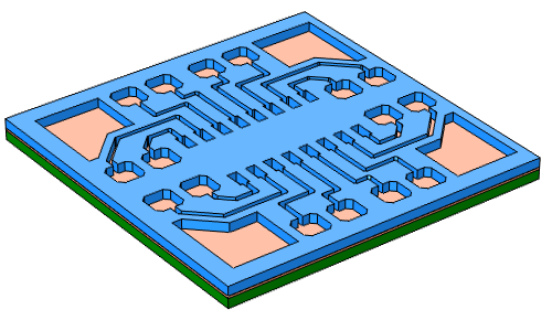
A seed layer is applied to the PCB (left). The PCB patterned with a photoresist using photolithography (right).
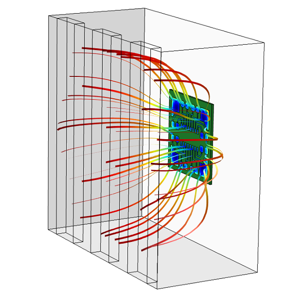
During the electroplating process, the PCB is submerged into an electroplating bath, which is an electrolyte containing sulphuric acid and copper sulphate, together with copper anodes (e.g., solid copper bars). A voltage is applied between the anodes and the seed layer, the cathode, which results in the electrochemical reduction of the copper ions to copper metal that is plated (deposited) on the seed layer. The thickness of the deposited layer is directly proportional to the rate of the electrochemical reaction over time, which is given by the current density at different positions in the seed layer over time. As a result, the patterned photoresist’s cavities are filled with solid copper. The plating rate is maintained by controlling the average current density (i.e., the total current over the pattern area to be plated).
Finally, the remaining photoresist is stripped away and the thin seed layer is etched to isolate the plated copper wires from each other.
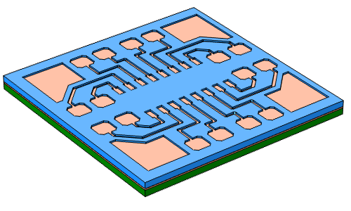
Copper is electrodeposited on the conducting seed layer, thereby filling up the patterned photoresist’s cavities on the PCB (left). The photoresist is stripped away and the exposed seed layer is etched to isolate the copper wires from each other (right).
Plating Rate Uniformity
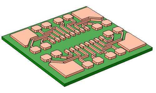
A known issue with this process is that the plating rate is not always uniform across the entire PCB. The electric field in the electrolyte is concentrated to the conducting pattern that is surrounded by large insulating areas, as well as in the pattern close to the PCB’s edges. These nonuniformities in the electric field lead to locally higher current densities at the surface of the cathode in those areas — an effect commonly referred to as current crowding. The plated thickness is proportional to the current density over time, which results in an unwanted thickness variation of the copper wires across the PCB. This means that there will be a resistance variation between copper wires in different positions in the PCB. That variation can be the root cause of performance issues or, in the worst case scenario, device failure when the PCB is used in an electronic device.
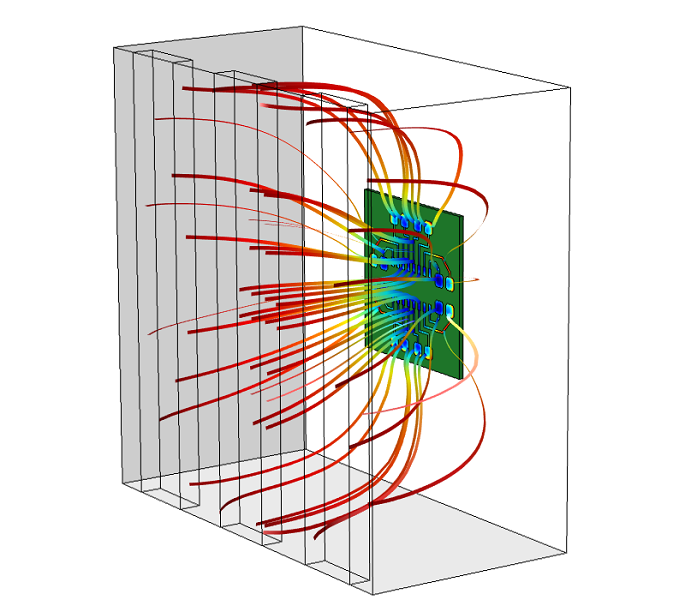
During the copper pattern plating step, the PCB is submerged into an electroplating bath (an electrolyte) together with copper anodes (left). When a voltage is applied between the anode and the PCB, copper is deposited to form the wire pattern. The electrical field from the anode to the conducting parts on the PCB is crowded in the pattern that is close to the large insulating areas and the edge of the PCB (illustrated by the colored electric field streamlines in the image to the left). This leads to locally higher copper thickness in these areas (seen in the red-colored parts of the wire pattern in the image to the right).
Simulations and Optimization in the Design Stage
To avoid reduced performance or device failure during the operation of electronic devices, the copper circuits must meet a set of thickness uniformity specifications. Normally, the printed circuit board designer would rely on simple design rules such as maximum and minimum lines, spaces, and pattern density. However, by using electroplating simulations, a much more accurate estimation of the expected copper thickness variation can be achieved. With this information, it is possible to modify the design at an early stage instead of waiting for prototype results.
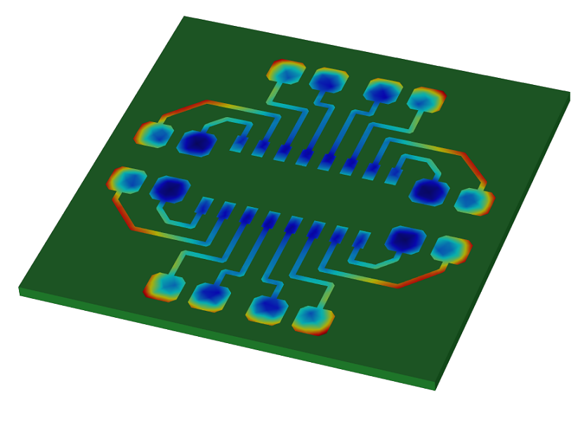
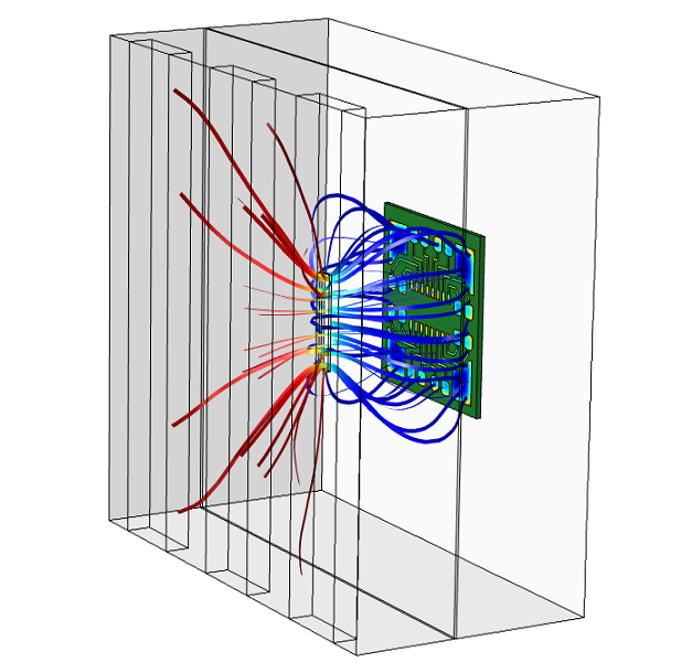
In order to reduce current crowding, a “dummy” pattern can be included in the design where there would normally be large insulating areas. In that case, the dummy pattern would receive some of the current, which reduces the high current density in the actual wiring pattern. Parts of the dummy pattern may still receive a high current density, but since it is not part of the actual wiring, this is not an issue. With simulations, it is fast and easy to redesign and evaluate the resulting thickness uniformity for different pattern layouts.
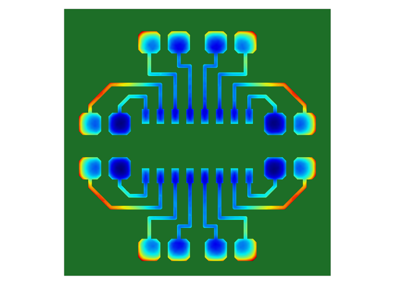
In order to reduce copper pattern thickness variation, a dummy pattern can be included where there would normally be large insulating areas. In the image to the left, the red-colored areas show the high thickness portions of the copper pattern that are close to insulating areas. The image to the right shows how a dummy pattern can be included to reduce the thickness variation in the copper wiring pattern.
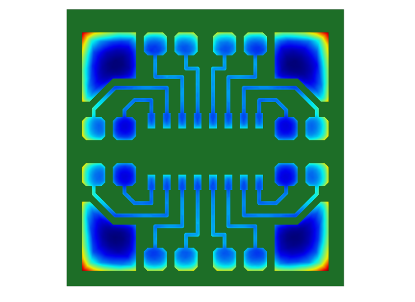
An additional step in reducing thickness variation is related to the set-up of the electroplating bath. To reduce the current crowding effect in the edges, a so-called aperture can be used.
The aperture is basically an insulating shield with an opening that is placed between the copper anodes and the PCB in the plating bath. The aperture opening must be smaller than the PCB dimensions in order to reduce the edge current crowding. Other than that, it is difficult to guess the optimal size and placement of the aperture.
Luckily, optimization through simulation is fairly quick and easy. In the illustrations below, an aperture with a rectangular opening is simulated. The length and width of the opening as well as the placement of the aperture in the bath are optimized to minimize the thickness variation across the PCB.
To avoid the current crowding effect close to the edge of the PCB and aperture (as seen in the left image), an insulating shield with an opening can be placed between the anodes and the PCB in the electroplating bath. The right image shows the aperture where the size of its opening and placement in the bath has been optimized using simulation to give the minimum thickness variation.
Manufacturing Cost Considerations
If PCB manufacturers want to be competitive, it is always essential to consider manufacturing costs. As mentioned above, there is usually a copper thickness uniformity specification that the final product needs to meet. The thickness uniformity is inherently dependent on the total plating rate used in the electroplating process; the higher the overall rate, the more thickness variation. Also, the total process time determines the throughput of the production line and, therefore, the manufacturing cost.
Minimizing Cost
To minimize the manufacturing cost, the process is run at the highest possible rate while still achieving the thickness specifications. By using simulations to study the impact of the plating rate, it is possible to estimate which plating rate can be run for a given thickness uniformity specification. This enables the estimation of the manufacturing cost in the design phase.
By improving the design or using an aperture to improve the uniformity, it is possible to simulate how much of a higher plating rate this would enable as well as how much money would be saved during PCB production.
Making Simulations Available with an Electroplating App
Electroplating simulation models are created by people with electrochemistry backgrounds and an understanding of simulation models and software. The PCB designer is normally skilled in electric design but has little or no knowledge about the electrochemical process that goes on during manufacturing.
Many of the benefits of electroplating simulations have been discussed, but how do you make the simulation models available for PCB designers?
Building an Application
One solution is to build an electroplating app with a tailored easy-to-use interface that allows PCB designers to study important parameters and run simulations with a few simple clicks.
With the Application Builder in COMSOL Multiphysics version 5.0, simulation experts can create these kinds of apps with very little effort and make simulations available to other stakeholders in an organization.
An electroplating app allows the PCB designer to import different designs (with or without dummy patterns), click Compute, and visualize the simulated thickness uniformity. It is also possible to change the dimensions of the plating bath and anodes as well as include an aperture. With a simple click, the app can also be run to optimize the dimensions and placement of the aperture. Finally, the app can be used to find out the maximum plating rate for a given thickness uniformity specification. With this information, the manufacturing cost can be estimated.
")
The user interface from an electroplating app. It allows PCB designers to upload different designs, modify the dimensions of the electroplating bath, and (optionally) include an aperture with certain dimensions.
")
With an electroplating app, a user can run a simulation with a simple click. Users can study the copper wire thickness uniformity and how it is affected by different designs, plating rates, and plating bath set-ups. Moreover, the app can also be run to simulate the optimal aperture dimensions for reducing thickness variation. Finally, the app can be used to calculate the maximum plating rate for a given thickness uniformity target.
Concluding Remarks
We have discussed the importance of simulations for advanced PCBs that use copper pattern electroplating technology. By running electroplating simulations in the design stage, reduced performance or even device failure caused by unwanted thickness variation in the electroplating process can be mitigated.
Traditionally, these kinds of simulation models would not be carried out by PCB designers and are more likely to be ran by electroplating and simulation experts. However, by building an electroplating app with a tailored easy-to-use interface, we can bring electroplating simulations to PCB designers. The designers will be able to run and utilize all of the benefits of simulation in their daily work.
In the end, money can be saved by reducing the number of prototypes and optimizing the design and process to minimize manufacturing costs. Further, similar apps can be incorporated into the manufacturing process and run by the engineers and technicians responsible for this process. This allows them to make small tweaks and calibrations to the operation of the electroplating as well as assist in quality assurance.


Comments (0)