
When a plane wave of electromagnetic radiation, e.g., light, is incident upon a planar periodic structure, higher-order diffraction may occur. This means that the light will not only reflect and refract according to Snell’s law, but it can also be scattered into multiple distinct directions, called the diffraction orders. Using a geometric approach can help us understand when these will be present and in which directions the light will scatter. Let’s learn more!
Understanding Diffraction from Planar Periodic Structures
We will consider here a plane wave of light incident upon a structure that is infinitely periodic in a plane. The media above and below the plane can have different refractive indices and are assumed to be lossless and of infinite extent. At the plane of the interface between these media, there can be periodic structures of any complexity in terms of material properties and shape, as long as these repeat periodically in the plane. Light that is incident onto such a structure will at least experience specular reflection; the light can also experience refraction (also called specular transmission) and often also some loss as electromagnetic energy is converted into heat. The angles of reflection and refraction are given by Snell’s law, but computing the fraction of the incident light that is reflected, transmitted, or dissipated within the periodic structure requires numerical analysis.
A plane wave incident at an angle upon a planar periodic structure. One unit cell of the periodic structure is highlighted.
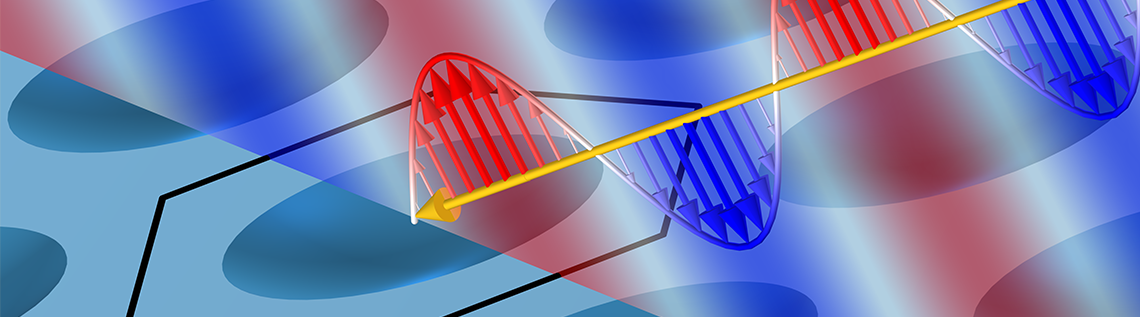
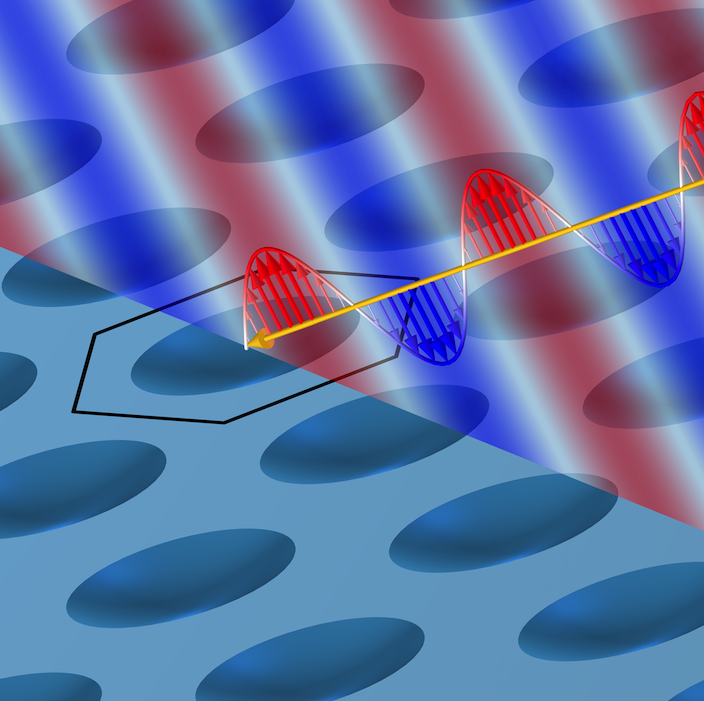
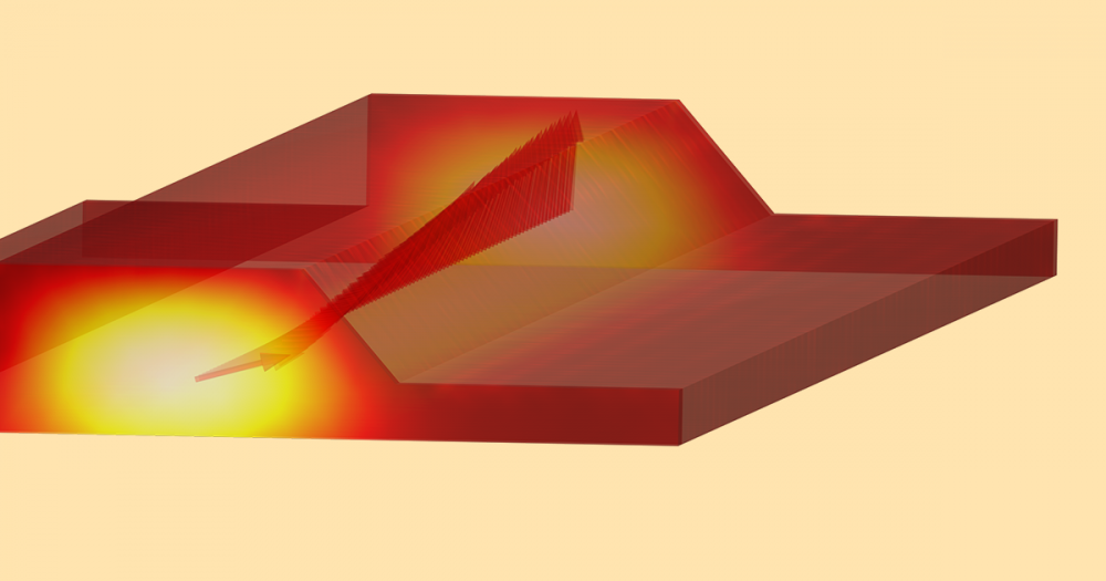
As noted, there is also the possibility of higher-order diffraction. This occurs when the light being scattered by the periodic structure interferes constructively into distinct directions. A sample of such a result is illustrated below.
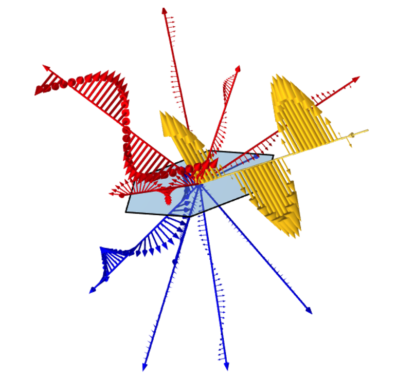
Illustration of a linearly polarized plane wave (yellow) incident upon a periodic unit cell. The incident light is scattered into several different diffraction orders with different intensities and polarizations in reflection (red) and transmission (blue).
Determining the fraction of light going into these other directions similarly requires building a numerical model, but understanding which directions the light will scatter into can be done with a purely geometric approach, called an Ewald sphere construction. It is helpful to be familiar with this approach prior to starting your numerical analysis, and that is what we will show here. The Ewald sphere geometric construction can be used both for planar structures with periodicity in one direction and for those with periodicity in two directions in the plane.
Structures with Periodicity in One Direction
Some planar periodic structures, such as gratings, have periodic variation in only one direction, meaning that there is no variation in the structure along the third dimension. When the incident light is propagating in the plane normal to this third dimension, the modeling can be reduced to a two-dimensional plane, with periodicity along one direction.
Plane wave incident at an angle upon a structure with periodicity in one direction, with no variation in the structure or fields along the out of plane direction. One unit cell is highlighted.
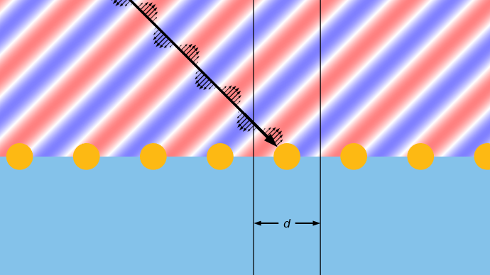
For these structures, we only need to consider the unit cell spacing, d, and begin by drawing a set of lattice points in reciprocal space, so the dimensions in the following figure have units of inverse length. The line of these lattice points corresponds to the plane of the interface of the periodic structure. The spacing between the lattice points is 2\pi/d, and the points are indexed starting from the zeroth lattice point, m=0, which can be thought of as sitting at the middle of the unit cell. Next, two semicircles are drawn above and below the line of the lattice points. These have a radius of n_{r}2\pi/\lambda_{0} on the reflection side and n_{t}2\pi/\lambda_{0} on the transmission side, where n_{r} and n_{t} are the refractive indices on the respective sides and \lambda_{0} is the free space wavelength. For incident light coming at an angle of \theta_{inc} from the normal, the common center of these circles are offset from the zeroth lattice point by sin(\theta_{inc})n_{r}2\pi/\lambda_{0}. The lattice points that lie within these semicircles correspond to the possible diffraction orders.
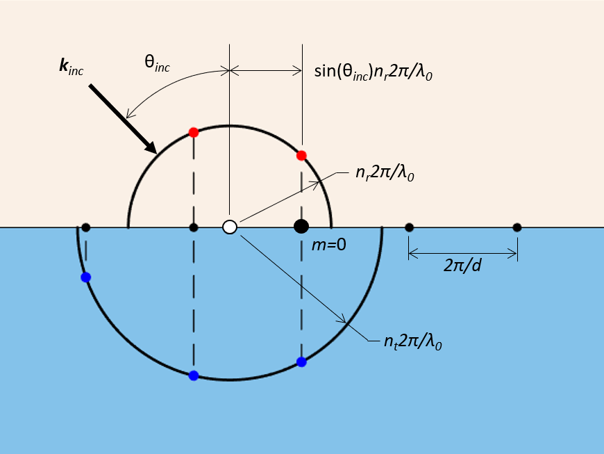
The geometric construction used to determine the diffraction orders from a planar structure with periodicity in one direction that is illuminated by a plane wave incident at an angle. Note how the center of the semicircles (white dot) are offset from the zeroth lattice point.
This construction can also be used to determine the directions into which the diffraction will occur and assign an indexing to each. The vectors from the center of the semicircles to the projection of the lattice points correspond to the \textbf{k}-vectors of each diffraction order. The indexing of these lattice points is of opposite sign on the two sides. The arrows to the zeroth lattice points will always be present; they represent specular reflection and transmission. The presence of other diffraction orders depends upon wavelength, refractive indices, spacing, and incident angle. Two examples of setting up this type of model are shown in the Application Gallery entries: Plasmonic Wire Grating (RF), which uses the RF Module, and Plasmonic Wire Grating (Wave Optics), which uses the Wave Optics Module.
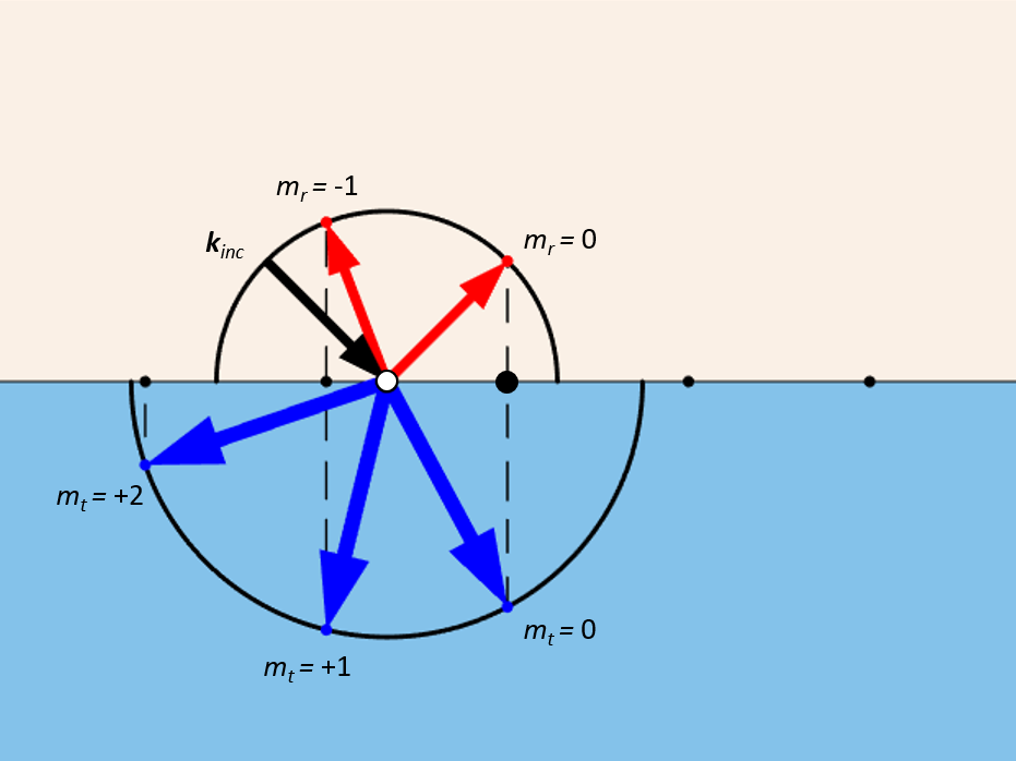
The wave vectors of the various diffraction orders from a planar structure with periodicity in one direction. Note the switch in sign of the indexing between the reflection and transmission diffraction orders.
Structures with Periodicity in Two Directions
Now let’s move on to the case of diffraction from a planar structure with periodicity in two directions in the plane. The figure below shows rectangular, rhomboidal, and hexagonal unit cells patterning a plane. These are defined by two unit cell vectors, \textbf{a}_{1} and \textbf{a}_{2}, that start at one point and follow the adjacent edges to the next vertex. Although we are free to work with any coordinates and orientation that we want, for the purposes of this blog post, we will choose to always have the \textbf{a}_{1} vector aligned with the global Cartesian x-axis and to always be looking down onto the unit cell from the direction of illumination. There are also two basis vectors, \textbf{b}_{1} and \textbf{b}_{2}, that describe how the unit cell has to be shifted in the plane to produce the tiling pattern. That is, patterning the entire plane involves copying the unit cell by m\textbf{b}_{1}+n\textbf{b}_{2} for any integer values of m and n. The magnitude of the cross product of these two vectors is used to find the area of the unit cell: A_{c} = ||\textbf{b}_{1}\times\textbf{b}_{2}||.
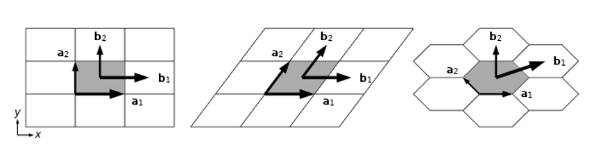
The rectangular, rhomboidal, and hexagonal unit cells pattern the two-dimensional plane. The unit cell vectors correspond to two edges of the cell, and the basis vectors describe how the cells need to be shifted to pattern the plane.
These basis vectors are used to define two reciprocal space diffraction vectors: \textbf{d}_{1} = 2\pi(\textbf{b}_{2} \times \textbf{n})/A_{c} and \textbf{d}_{2} = 2\pi(\textbf{n} \times \textbf{b}_{1})/A_{c}, where \textbf{n} = (\textbf{b}_{1} \times \textbf{b}_{2})/A_{c} is the normal vector to the plane of periodicity, the +z-axis. These diffraction vectors are perpendicular to the basis vectors and are used to create a diffraction lattice in the plane of periodicity by taking integer sums: m\textbf{d}_1+n\textbf{d}_2, with each point in the lattice corresponding to an index pair of m and n in the \textbf{d}_{1} and \textbf{d}_{2} directions. On the transmission side of the unit cell, the points are at the same locations but the indices are switched and have opposite sign.
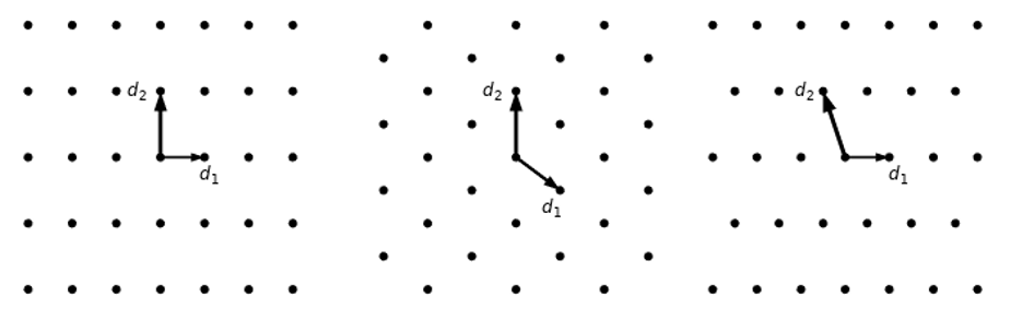
The diffraction vectors and lattice points plotted in reciprocal space.
We can now visualize these diffraction points on the plane of periodicity in 3D space and add a hemisphere of radius equal to the wave vectors in the material above and below the plane. These hemispheres inform us of which diffraction orders are present in reflection and transmission. We initially center this sphere at the m = 0, n = 0 point, representing normally incident light.
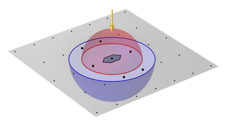
Plane wave light (yellow arrow) normally incident upon a periodic hexagonal unit cell. The diffraction points are plotted in the plane of periodicity, and the highlighted points that lie within the reflection and transmission hemispheres indicate which diffraction orders will be present.
Next, we consider what happens as the elevation and azimuthal angle of incidence are varied. Keeping in mind that we choose the convention of keeping the \textbf{a}_{1} vector aligned with the global +x-axis, increasing the elevation angle of incidence means that the incident wave vector is first rotated about the –y-axis; then, an increase in the azimuthal angle of incidence applies a subsequent rotation about the +z-axis. So, the elevation angle of incidence goes from 0^{\circ} \le \alpha_{1} < 90^{\circ}, and the azimuthal angle of incidence goes from 0^{\circ} \le \alpha_{2} < 360^{\circ} , as visualized below. The incident wave vector, along with the normal to the plane of periodicity, defines the plane of incidence. The plane of incidence is defined as the xz-plane for the case of normal incidence: \alpha_{1} = 0^{\circ}, \alpha_{2} = 0^{\circ}.
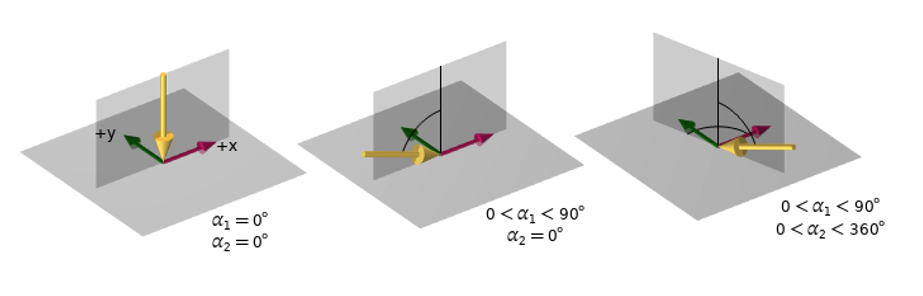
The elevation and azimuthal angles of incidence represent a set of sequential rotations of the incident wave vector (yellow), first about the –y-axis and then about the +z-axis. The plane of incidence is also shown.
These changes to the incident angles change the position of the center of the hemispheres. The distance in reciprocal space from the hemisphere center to the m = 0, n = 0 point is k_{r} = \text{sin(}\alpha_{1}\text{)}2π/ \lambda_r, and the position is shifted in the plane by k_{x} = -k_{r}\text{cos(}\alpha_{2}\text{)} and k_{y} = -k_{r}\text{sin(}\alpha_{2}\text{)}, as shown below. So, a change in elevation angle and azimuthal angle often leads to a different set of diffraction orders being present.
Plane wave light incident at a nonzero elevation and an azimuthal angle of incidence shift the center of the hemispheres so a different set of diffraction orders are present.
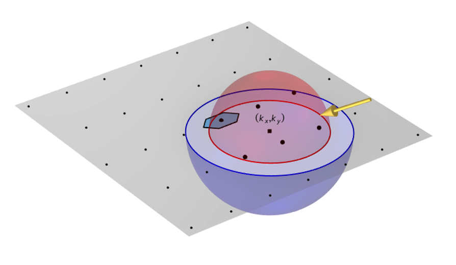
These hemispheres also tell us the wave vectors of each diffraction order. Projecting the diffraction order points onto the hemispheres, we get another set of points, and the wave vectors of each diffraction order are equal to the vectors from the hemisphere center to these projected points.
Projecting the diffraction points onto the hemispheres gives the wave vector of each diffraction order. This geometric construction illustrates into which directions the incident light (yellow) will be diffracted upon reflection (red) and transmission (blue). You can interact with this 3D model with your mouse: left-click to rotate, right-click to pan, and scroll wheel to zoom.
Finally, these vectors also inform us about how the polarization state will be reported. For each diffraction order, a polarization state is reported in terms of the in-plane and out-of-plane components of the Jones vector. The plane of each diffraction order is the plane described by the wave vector and the normal vector to the plane of periodicity. The out-of-plane component of the Jones vector, for all diffraction orders, corresponds to a wave with the electric field parallel to the plane of periodicity.
The diffraction order directions describe a set of planes that are used to define the polarization state of each diffraction order. The plane of incidence and one diffraction order are highlighted. You can interact with this 3D model with your mouse: left-click to rotate, right-click to pan, and scroll wheel to zoom.
Conclusion
We have reached the conclusion of the geometric construction using the Ewald sphere to understand diffraction from planar periodic structures, and we can see that this tells us which higher diffraction orders will be present in reflection and transmission. It also tells us their wave vectors and the set of planes used for defining the orientation of the Jones vectors. We get all of this information automatically when solving a numerical model, so this kind of geometric construction isn’t necessary to go through, but it can be helpful in building up our understanding and intuition.
Further Learning
If you’d like to get started with modeling higher-order diffraction, the following example models, which can be built with the RF Module or Wave Optics Module, are good starting points.
- Models built with the RF Module:
- Models built with the Wave Optics Module:

Comments (0)