

When designing piezoresonators for modern communication systems, a high-fidelity multiphysics simulation is absolutely indispensable to capture complex device behavior. However, in real-world RF front ends, you often need to chain dozens of components together or construct external matching networks. In that case, running a full-fledged finite element method (FEM) simulation is computationally demanding. The modified Butterworth–Van Dyke (mBVD) equivalent circuit solves this issue. By condensing finite element data into a compact lumped model, you unlock near-instantaneous system simulations without sacrificing physical accuracy.
The Resonator Essentials: Physics, Admittance, Damping, and Electromechanical Coupling
Before we dive into the circuit formalism, I will set the scene from a physics standpoint. A standard bulk acoustic wave (BAW) or surface acoustic wave (SAW) resonator uses the piezoeffect to trap acoustic energy at natural frequencies inside a microscale cavity. To analyze this behavior from the electrical point of view, we track terminal admittance, Y=I/V , where its:
- Real part, conductance, G=real(Y) , represents energy transfer
- Imaginary part, susceptance, B=imag(Y) , tracks energy storage
This electromechanical interaction yields two primary frequencies. At the series resonance frequency f_s , standing acoustic waves constructively interfere. Internal mechanical impedance drops to a minimum, causing a sharp peak in electrical conductance B . The antiresonance or parallel resonance frequency f_p is located slightly higher. Here, the piezoelectrically generated charge from mechanical strain cancels out the electrostatic plate charge on the electrodes. The device draws minimal net current, driving the total admittance magnitude to a minimum.
The gap between f_s and f_p defines the effective electromechanical coupling coefficient k^2_{eff}, which is a measure of the energy conversion efficiency: k^2_{eff} \propto (f_p^2 – f_s^2)/f_s^2. A larger frequency split provides a higher k^2_{eff}, directly translating to a wider achievable filter bandwidth. The exact definition of the effective electromechanical coupling coefficient depends on the standard or approximation you follow. The formula may deviate a bit between BAW and SAW applications or if your conditions satisfy the small-coupling approximation.
In an ideal lossless resonator, the conductance peak at f_s would approach infinity, and the admittance valley at f_p would drop to absolute zero. Real-world piezoelectric devices, however, experience energy dissipation due to internal material damping, both mechanical and dielectric, as well as other mechanisms, such as anchor leakage into the substrate. This total dissipation dictates the device’s Q factor, Qf . On the admittance curve, higher material damping directly suppresses and flattens the response. It rounds off the sharp resonance peaks and valleys, lowering the maximum conductance at f_s and raising the minimum admittance floor at f_p . For RF filter designers, minimizing this damping to achieve a high Q factor is essential to ensure low insertion loss and steep filter skirts.
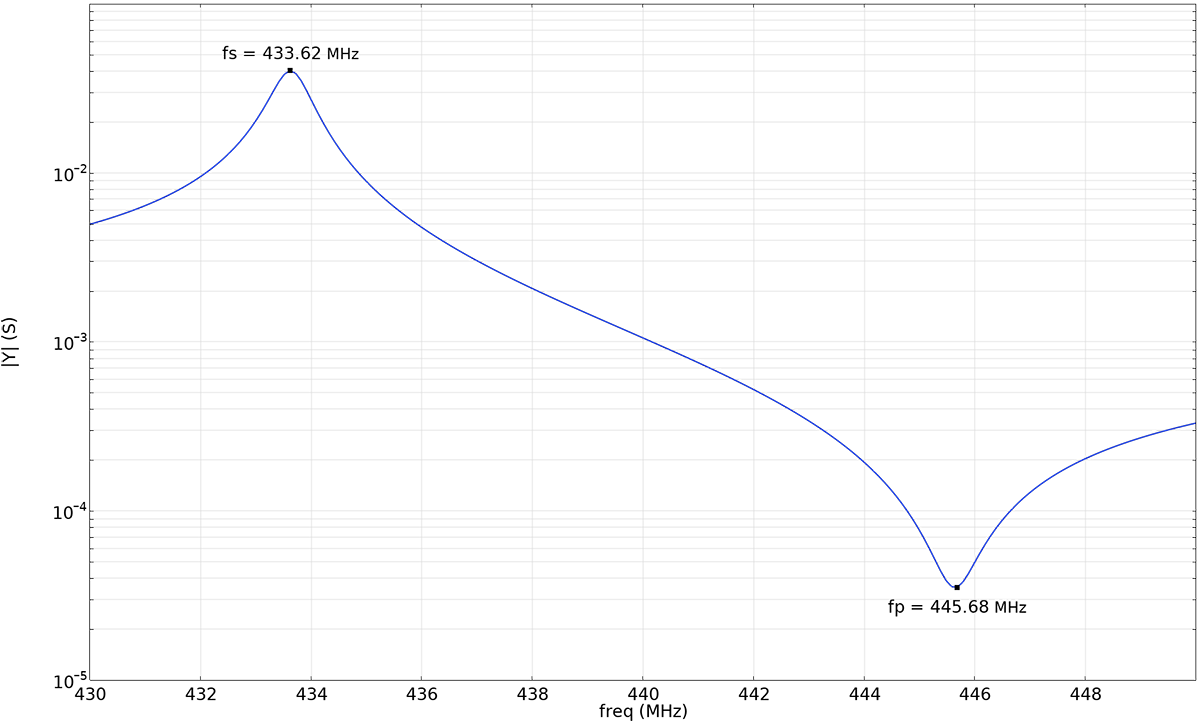
A convenient admittance magnitude |Y| curve sketch with the series resonance and parallel antiresonance points mapped out.
Representing a Piezoelectric Resonator in a FEM Manner
If you were to create a representative FEM model of a piezoelectric resonator, it would be straightforward in COMSOL Multiphysics® and reveal the powerful multiphysics capabilities of the software. The steps are as follows: Start with a Piezoelectricity interface that couples an Electrostatics interface with a Solid Mechanics interface. For Solid Mechanics, select the Piezoelectric Material material model and specify the relevant lossy behavior through its subnodes, such as Mechanical Damping and Dielectric Loss.
To run a Frequency Domain study, you might want to drive your device via a Terminal condition, added in the Electrostatics interface. Among other benefits, this feature automatically derives the terminal admittance, making it readily available for plotting and further results evaluation. The results evaluation includes extracting the mentioned resonance frequencies and Q factors. Alternatively, you may opt for an Eigenfrequency analysis, which also helps retrieve resonance frequencies and Q factors.
Bridging Finite Elements and Lumped Parameters
The beauty of a lumped-parameter circuit model lies in its simplicity, as solving a network of a few resistors, inductors, and capacitors takes fractions of a second but still provides you with the sought admittance curve. The electromechanical equivalent framework, which is central to this blog post, traces its lineage back to Stephen Butterworth’s filter designs and Walter Guyton Van Dyke’s early-20th-century work mapping the behavior of quartz crystals. The “modified” modern version adds parasitic elements to fit the stringent demands of high-frequency MEMS resonators.
Modern RF MEMS resonators demand an engineering synergy between fast circuit models and modern numerical solvers. A circuit model is only as good as its input parameters. You cannot simply guess the equivalent capacitance of a complex, layered SAW interdigital finger topology or the motional resistance of a novel piezoelectric thin film. By using COMSOL Multiphysics® to simulate the true geometric and material complexities of your device, you can extract the exact lumped parameters needed to populate your mBVD circuit. Altogether, the FEM provides the ground-truth physics, while the circuit representation allows for the system-level speed.
Note: The classic mBVD model configuration to be discussed here is chiefly designed for one-port resonators featuring a single signal terminal and a ground terminal. If your design boils down to a multiport configuration or the like, you will need to expand this framework into a more elaborate one.
Similarly, for the sake of clarity, we will focus on one particular resonance. You will need to add an extra parallel motional branch for every resonance mode you need to consider.
Breaking Down the mBVD Circuit
The conventional mBVD model captures a standard piezolelectric resonator behavior by splitting the electrical behavior after the initial series routing into two parallel paths: a static branch representing the physical dielectric layer stackup and a motional branch representing the electromechanical acoustic resonance. A circuit schematic is provided below.
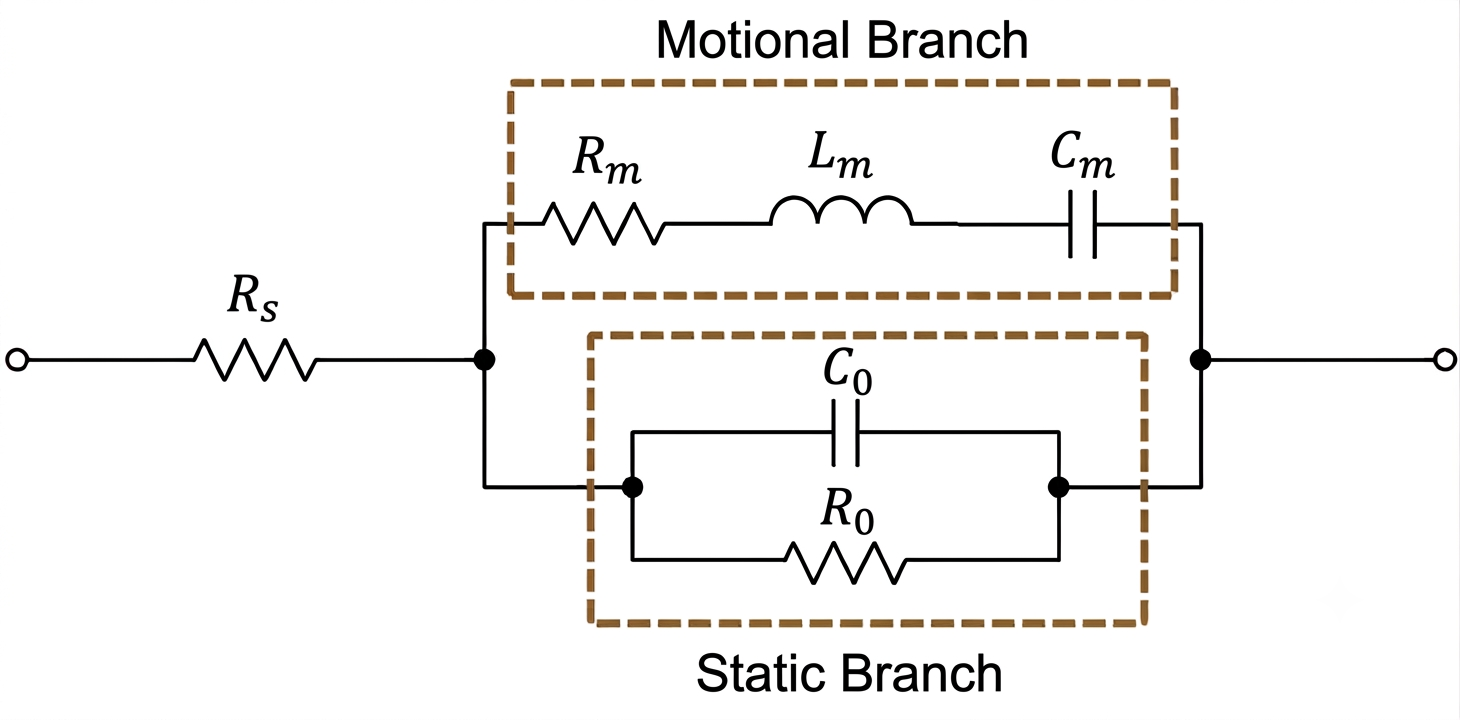 A schematic of the one-port mBVD circuit topology showing the series resistance, R_s , connected to the parallel combination of the motional and static branches. The motional branch includes R_m , L_m , and C_m , which form a series contour, and the static branch includes C_0 and R_0 , which are connected in parallel.
The table below can be used to consider each element, how the elements impact the electrical admittance response, and how to cleanly extract their values from your FEM simulation.
| Circuit Element | Physical Meaning | Admittance Impact | How to Extract It |
|---|---|---|---|
| Series resistance,R_s | This element represents the purely ohmic resistance of the metal electrodes, busbars, and interconnect wires leading up to the active area of the resonator. | It limits the maximum peak of the admittance magnitude at series resonance f_s. | R_s can be calculated directly from the conductivity and geometry of the metal routing in your model, say via an auxiliary Electric Currents setup. You typically don’t need to include it explicitly in your main Piezoelectricity simulation. |
|
Static capacitance, C_0 |
C_0 represents the electrical plate capacitance, which is formed by the overlapping electrodes and the intervening piezoelectric material. C_0 is independent of mechanical movement. | It establishes the baseline “floor” of the imaginary admittance curve and determines the frequency separation between your series resonance f_s and parallel antiresonance f_p. | Run a frequency-domain simulation at an arbitrary point, f_l, well below f_s, where the device is mechanically “dead” and the motional branch acts as an open circuit. Evaluate the imaginary part of the admittance to isolate the static capacitance as C_0=B(f_l)/(2 \pi f_l) |
| Static resistance, R_0 | R_0 represents the bulk dielectric material losses and electrical leakage paths through the piezoelectric layer. | It introduces a clean, flat baseline conductance to the real part of the admittance curve at low frequencies. | Assuming that your model goes with a nonzero dielectric loss, in the same low-frequency regime used to find C_0, i.e., well below acoustic resonance, measure the real part of the admittance to directly isolate the flat baseline dielectric leakage as R_0=1/G(f_l). For a case of small dielectric loss, R_0 is supposed to get a huge value. |
| Motional capacitance, C_m | This element represents the mechanical elasticity or compliance of the resonator structure, which is intimately tied to the effective electromechanical coupling coefficient k^2_{eff} of the piezoelectric crystal. | It dictates the overall strength of the resonance. A higher coupling coefficient increases C_m. Subsequently, it widens the window between f_s and f_p, which is a vital feature for wide-bandwidth RF filters. | C_m can be pulled instantly using your extracted C_0 value and the resonance frequency ratio via C_m=C_0 ( f_p/f_s)^2-1). |
| Motional inductance, L_m | This element represents the effective acoustic mass or inertia of the vibrating crystal lattice or thin-film membrane. | Together with C_m, it determines the exact frequency location of the series resonance peak. This calculation follows the classical formula for resonance frequency f_s=1/ (2 \pi \sqrt{L_m C_m}). | Once you know C_m and have identified f_s from your simulation data, you can define the motional inductance as L_m=1/((2\pi f_s)^2 C_m). |
| Motional resistance, R_m | This resistance accounts for the total mechanical and acoustic energy dissipation in the device. | It dictates the height and sharpness of the admittance peak at resonance. A lower R_m value signifies lower loss, leading to a much higher Q factor. | In the Frequency Domain sweep, the peak admittance at f_s is dominated by the motional branch. The peak conductance simplifies to R_m \approx 1/G(f_s). Alternatively, you can pull the device’s mechanical Q factor, Q_{fm}, from the Eigenfrequency study and use the following relation: R_m = \sqrt{L_m/C_m}/Q_{fm}. |
Here we opted for the mBVD configuration featuring the static branch with C_0 and R_0 connected in parallel. The alternate convention with these elements connected in series also exists, and, if chosen, it will affect their extraction logic and interpretation. Two approaches are interchangeable in the sense that once the lumped parameters are obtained attentively, the outputs are to be identical.
Extracting the Parameters
Provided that we are now equipped with both theory and extraction logic, let’s extract the full set of lumped parameters and construct the mBVD circuit within COMSOL Multiphysics®.
Note that this blog post acts as the primary resource for this model. If you’re interested in finding step-by-step instructions for leveraging similar models and plotting admittance curves, check out the example models we have available for the MEMS Module.
Here, we opt for a 3D layered one-port thin-film bulk acoustic resonator (FBAR), shown below. We also assume that R_s is known beforehand and for further comparison, just add its contribution manually to the device’s admittance.
To accurately extract resonance frequencies and the peak conductance from the Frequency Domain study, you might want to refine the frequency step and use the Graph Markers for a Global admittance plot. Do not forget to assign the Dielectric Loss if you consider R_0. Finally, it makes sense to run a separate study for a frequency several orders smaller than f_s for the purpose of R_0 and C_0 extraction.
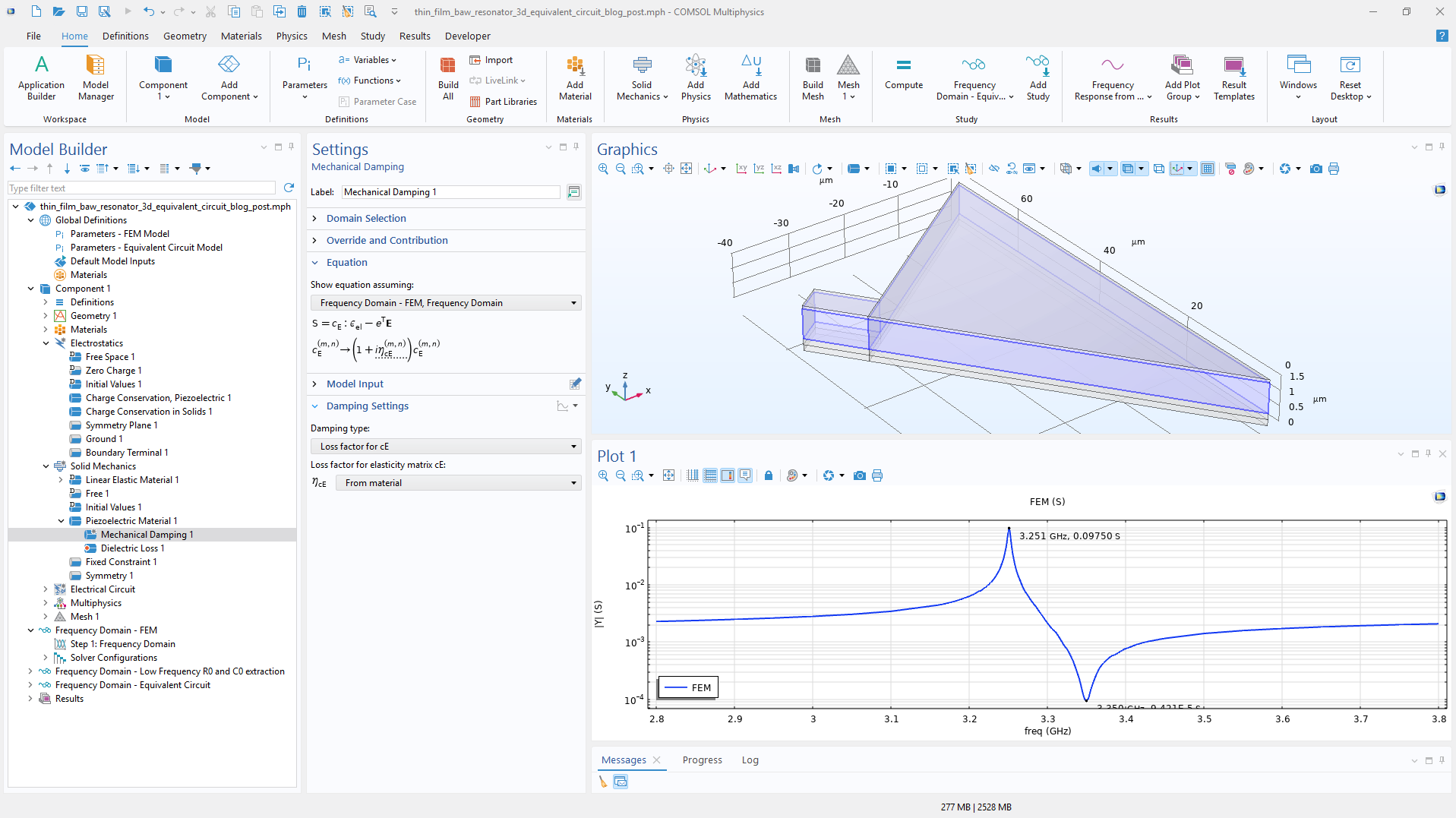 The UI in COMSOL Multiphysics® showing a 3D FBAR model, with its admittance calculated via the Frequency Domain study.
Once all the parameters are calculated, you can bring these values directly into the built-in Electrical Circuit interface within the same model file to verify your work. Connect your newly defined lumped mBVD circuit to a voltage source and overlay its impedance response directly onto your original FEM data. Following the modern and handy AI trends, do not hesitate to ask the optional Chatbot window in COMSOL Multiphysics® to provide you with COMSOL API code for adding the circuit with all the needed settings, as was done here.
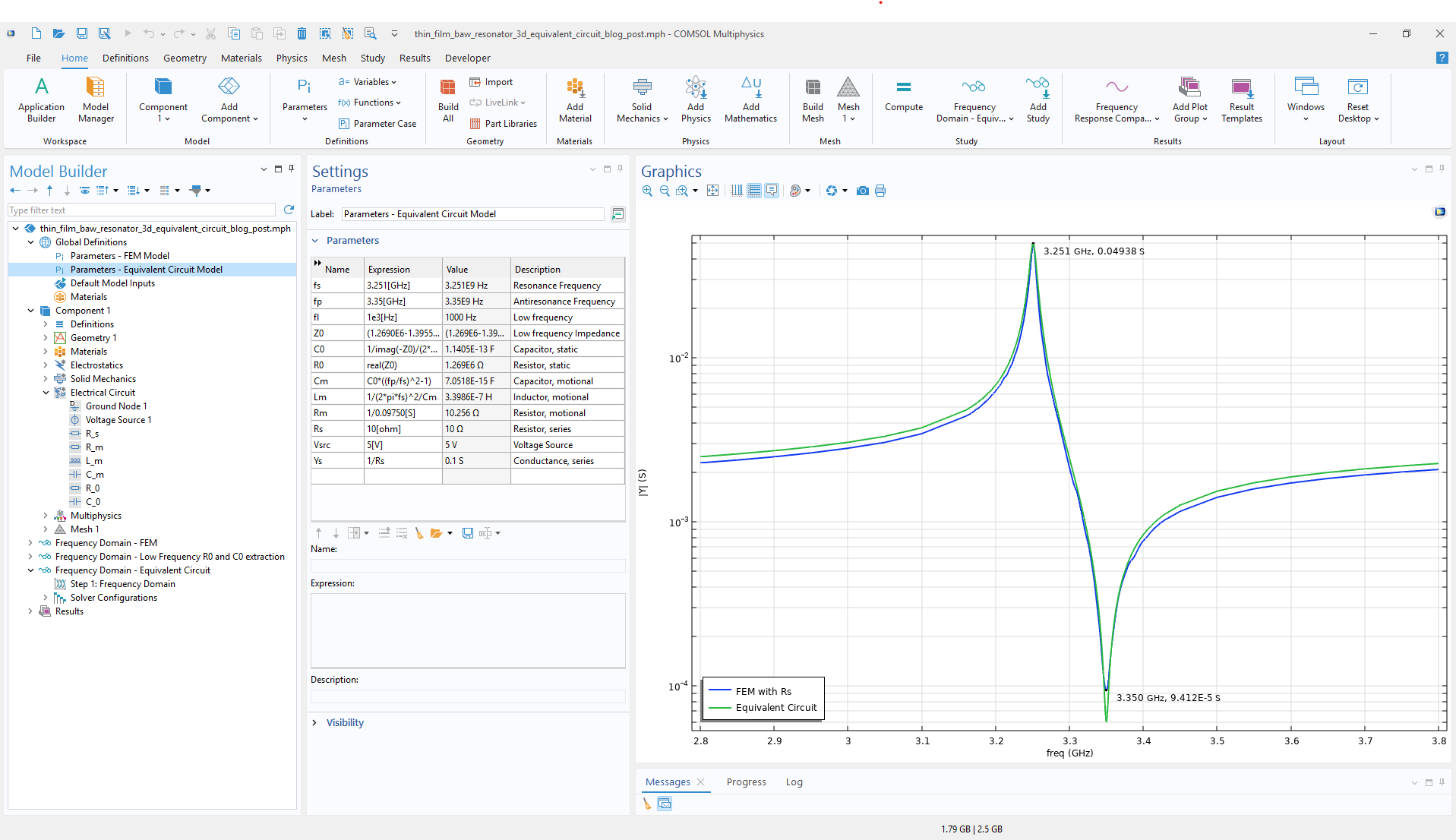 The extracted mBVD parameters for the Electrical Circuit interface and the plot depicting good correlation between the full-fledged FEM model and the circuit representation.
The result is a great match around the operational bandwidth. From any practical standpoint, a minor discrepancy can be explained by the fact that the FEM model captures contributions from high-order modes present in the system. Once your mBVD circuit block matches the physics-based model, you are no longer constrained by the physical geometry. You can extend the circuit network right inside COMSOL Multiphysics® by adding external tuning capacitors, inductors, or transmission lines, or by cascading multiple identical blocks to form complex ladder filters. Altogether, you end up with a verified, lightning-fast lumped model that seamlessly bridges microscale multiphysics with macroscopic system reality, enabling you to run massive sweeps in seconds.
Next Steps
Let’s wrap up by sharing the model featured in this blog post as well as related examples:
- Check out the model discussed in this blog post: Extracting mBVD Circuit Parameters from a 3D BAW Resonator
- To learn how to approach the same task from the Eigenfrequency side, see: Frequency-Domain Analysis of a SAW Unit Cell
- If you need a perfect match and/or a way to compensate for missing data (e.g., damping ratios), see this example, which makes use of the Parameter Estimation feature: Thin-Film BAW Resonator with Equivalent Circuit
- Check out tutorial models that leverage the MEMS Module: Application Gallery





Comments (0)