
Besi Improved Memory Chip Manufacturing with Multiphysics Simulation
Stefan Behler, Besi, Switzerland
As memory chips become smaller and smaller, designers must ensure that the chips stay intact during the manufacturing process. Besi develops equipment and assembly processes for substrate and wafer packaging production in markets such as consumer electronics, automotive, industrial, and solar energy. Stefan Behler, a senior expert process engineer, used multiphysics simulation to explore and optimize a new way of peeling off the tape on a memory chip that results in less deformation of the dies. This new method is now used by semiconductor packaging factories all over the world.
Suggested Stories
Understanding Brillouin Optomechanical Interaction with Multiphysics Modeling
Researchers from the University of Campinas and Corning wanted to see how photoelastics and moving boundary effects ...
Optimizing a CVD Process for a High-Performance Tungsten Material
Researchers at Forschungszentrum Jülich GmbH, Institute for Energy and Climate Research, and Max Planck Institute for ...
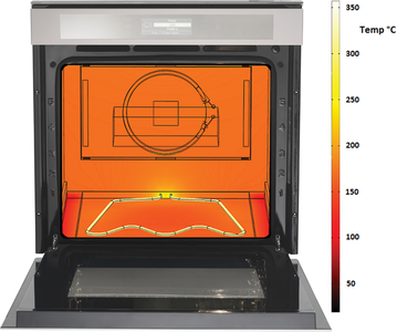
Simulation Turns Up the Heat and Energy Efficiency at Whirlpool Corporation
Engineers working on a joint research project between Whirlpool Corporation and the European initiative GREENKITCHEN ...
Keynote: Multiphysics Modeling in AR & VR Innovation
Meta is working to advance the optical and display technologies for its augmented reality (AR) and virtual reality ...


