La Galleria delle Applicazioni raccoglie un'ampia varietà di tutorial e di app dimostrative realizzati con COMSOL Multiphysics in diversi ambiti applicativi, inclusi quelli elettrico, meccanico, fluidico e chimico. E' possibile scaricare i file dei modelli e delle app demo pronti all'uso e le istruzioni step-by-step per costruirli, e utilizzarli come punto di partenza per le proprie simulazioni.
Lo strumento di Ricerca Rapida permette di trovare i modelli che si riferiscono alla propria area di interesse.
Si noti che molti degli esempi qui presentati sono accessibili anche tramite le Librerie delle Applicazioni incorporate nel software COMSOL Multiphysics® e disponibili dal menu File.
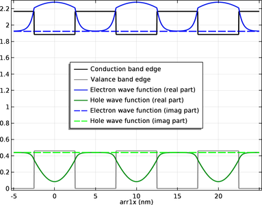
The Superlattice Band Gap Tool model helps the design of periodic structures made of two alternating semiconductor materials (superlattices). The model uses the effective mass Schrödinger equation to estimate the electron and hole ground state energy levels in a given superlattice ... Per saperne di più
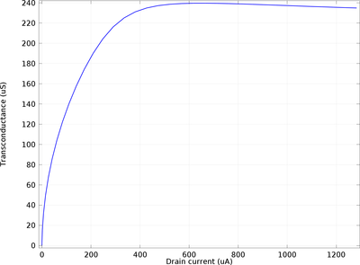
This model shows how to compute the AC characteristics of a MOSFET. Both the output conductance and the transconductance are computed as a function of the drain current. Per saperne di più

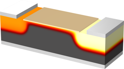
This model calculates the current and charge characteristics of a floating gate Electrically Erasable Programmable Read-Only Memory (EEPROM) device. A stationary study demonstrates the effects of varying the charge stored on the floating gate by computing Current-Voltage curves as a ... Per saperne di più
This example is an adaptation of our DC Characteristics of a MOS Transistor (MOSFET) model where the metal and dielectric domains are modeled explicitly and not via a boundary condition. Therefore, the potential profile inside the metal and the insulator can be observed. Per saperne di più

This tutorial simulates the turn-on transient (forward recovery) of a simple PIN diode, based on the book "Fundamentals of Power Semiconductor Devices" by B. J. Baliga (p. 242, 2008 edition). The diode is current driven with a constant ramp rate of 1e9, 2e9 and 1e10 A/cm^2/sec and a ... Per saperne di più
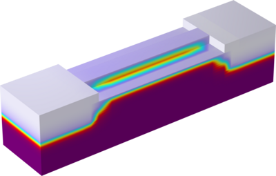
This example shows how to model a FinFET in 3D. The I-V characteristics of the device are simulated. First, the gate voltage is swept to obtain the drain current versus gate voltage plot. Then, the drain current versus drain voltage characteristics are computed for fixed gate voltages. Per saperne di più
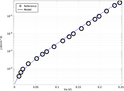
Schottky Contact This benchmark simulates the behavior of an ideal Schottky barrier diode made of a tungsten contact deposited on a silicon wafer. The resulting J-V (current density vs. applied voltage) curve obtained from the model under forward bias is compared with experimental ... Per saperne di più
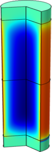
A gate-all-around MOSFET consists of a nanowire with a gate electrode wrapped around the circumference. Since the entire nanowire forms the channel, this configuration provides the best possible electrostatic control of the channel and offers a good candidate for the miniaturization of ... Per saperne di più

This example shows an approximate approach to model a dot-in-well solar cell as described by Asahi et al. in the reference paper. The quantum wells and the layers of quantum dots are each treated as lumped energy levels in the band gap. The authors specify transitions between the dot ... Per saperne di più
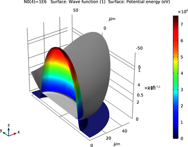
This tutorial model solves the Gross–Pitaevskii Equation for the ground state of a Bose–Einstein condensate in a harmonic trap, using the Schrödinger Equation interface in the Semiconductor Module. The equation is essentially a nonlinear single-particle Schrödinger Equation, with a ... Per saperne di più