La Galleria delle Applicazioni raccoglie un'ampia varietà di tutorial e di app dimostrative realizzati con COMSOL Multiphysics in diversi ambiti applicativi, inclusi quelli elettrico, meccanico, fluidico e chimico. E' possibile scaricare i file dei modelli e delle app demo pronti all'uso e le istruzioni step-by-step per costruirli, e utilizzarli come punto di partenza per le proprie simulazioni.
Lo strumento di Ricerca Rapida permette di trovare i modelli che si riferiscono alla propria area di interesse.
Si noti che molti degli esempi qui presentati sono accessibili anche tramite le Librerie delle Applicazioni incorporate nel software COMSOL Multiphysics® e disponibili dal menu File.
This model shows how to set up a 3D simulation of a n-p-n bipolar transistor. It is a 3D version of the device shown in the Bipolar Transistor model, and demonstrates how to extend semiconductor modeling into 3D using COMSOL Multiphysics. As in the 2D version of this model, the device ... Per saperne di più

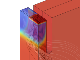
This benchmark example builds two models of a cross-bridge Kelvin resistor used for extracting the specific contact resistivity. The first model simulates the system in 3D, using the contact resistance feature built in the Semiconductor interface. The other model is a 2D approximation of ... Per saperne di più
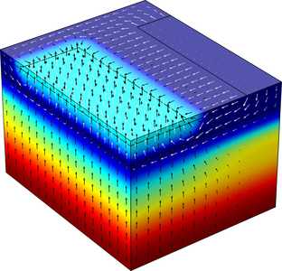
In this second half of a two-part example, a 3D model of a trench-gate IGBT is built by extruding the 2D model from the first half. Unlike the 2D model, now it is possible to arrange the alternating n+ and p+ emitters along the direction of extrusion as in the real device. This more ... Per saperne di più

This model shows how to set up a simple Bipolar Transistor model. The output current-voltage characteristics in the common-emitter configuration are computed and the common-emitter current gain is determined. Per saperne di più
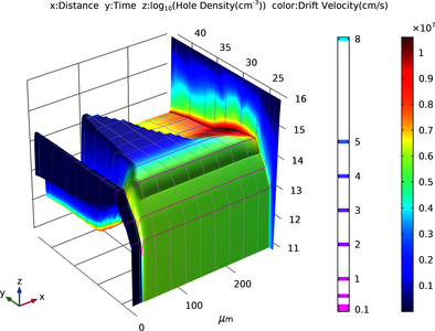
This tutorial performs steady-state and transient analysis of the response of a PIN diode to constant and pulsed radiation, respectively. The effect of radiation is modeled as spatially uniform generation of electron-hole pairs within the device. At high dose rates the separation of the ... Per saperne di più
This model shows how to model the avalanche breakdown due to the impact ionization in a Silicon Carbide diode. The current-voltage (I-V) characteristics of the device are presented as well as the electric field distribution plot. Furthermore, the carrier generation term has been computed ... Per saperne di più
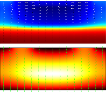
This model demonstrates how to couple the Semiconductor interface to the Heat Transfer in Solids interface. A thermal analysis is performed on the existing bipolar transistor model in the case when the device is operated in the active-forward configuration. The Semiconductor interface ... Per saperne di più
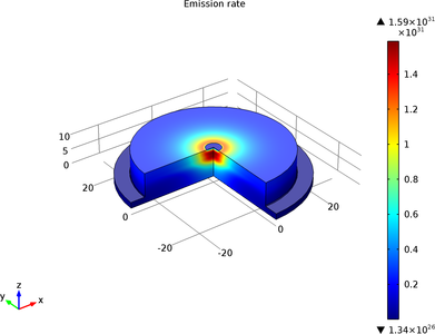
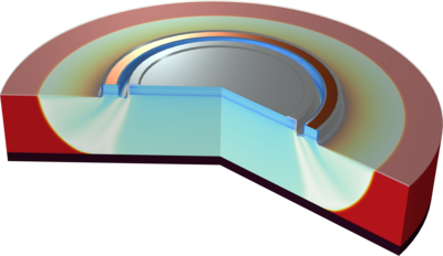
This model simulates an LED that emits in the infrared part of the electromagnetic spectrum. The device structure is made up of a single p-n junction formed by a layer of p-type doping near the top surface of an otherwise n-type wafer. This kind of device geometry is simple and cheap to ... Per saperne di più
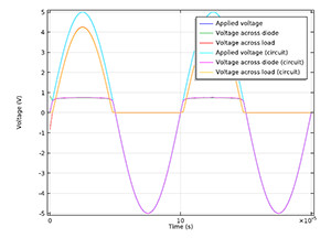
This model extracts spice parameters for a silicon p-n junction diode. The spice parameters are used to create a lumped-element equivalent circuit model of a half-wave rectifier that is compared to a full device level simulation. In this example, a device model is made by connecting a 2D ... Per saperne di più
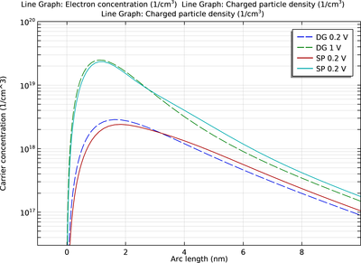
This tutorial demonstrates the use of the density-gradient formulation to include the effect of quantum confinement in the device physics simulation of a silicon inversion layer. This formulation requires only a moderate increase of computational resources as compared to the conventional ... Per saperne di più