
Sputtering is widely used in semiconductor processing to deposit uniform, thin, and well-adhered films on substrates. It can also be used for physical material removal in applications such as ion milling. In this blog post, we share an example of how modeling and simulation can be used to understand some of the phenomena involved in sputtering and help guide process development.
What Is Sputtering?
Sputtering is a physical process where ionized particles of a plasma or gas are bombarded on a solid surface, or target, to displace the target’s atoms, which can then land on another surface, or substrate. Sputtering occurs naturally in outer space and can be an unwelcome source of wear in precision components. However, it is also useful for thin-film deposition and for physical surface removal in semiconductor manufacturing, optics, and MEMS applications. A schematic of a sputtering setup can be seen in the figure below.
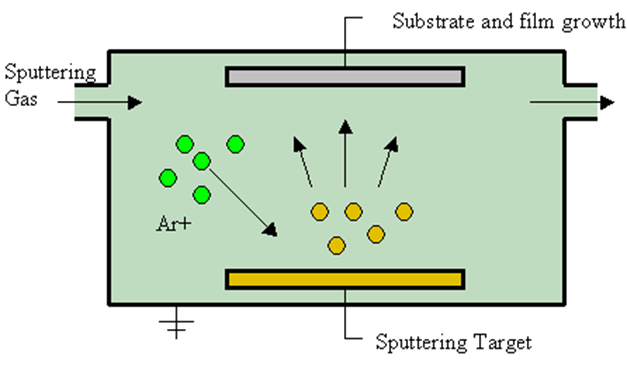 A typical sputter deposition setup. Image in the public domain, via Wikimedia Commons.
Various types of sputtering mechanisms, namely magnetron, reactive, and ion-beam sputtering, are used in the semiconductor industry to deposit thin films, which are crucial for creating the complex multilayer structure required in today’s integrated circuits. These films may form barrier layers, adhesion layers, or conductive layers within chips. Sputtering offers several advantages in this regard. For instance, it enables excellent control over the thickness of the deposited film while being applicable for different materials, such as metals, alloys, and compounds. Moreover, sputtering is the ideal choice for substrates that cannot withstand higher temperatures.
In addition to thin-film deposition, sputtering is also used for the selective removal of material from a wafer in dry etching by employing ionized gas particles guided by a protective mask. Inert gases such as xenon and argon are typically preferred as sputtering gases because of their minimal reactivity and ability to cause higher displacement of the target material due to their significant molecular weight.
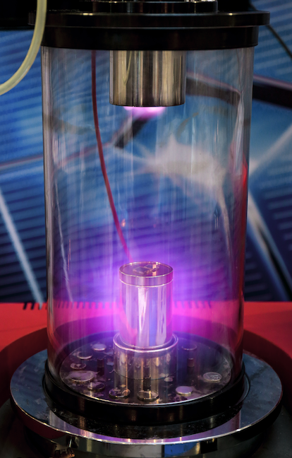
A sputtering device, with plasma in a vacuum glass tube.
Understanding Complexities with Simulation
While sputtering is commonly used in chip manufacturing and thin-film processing, complexities arise mainly due to various phenomena simultaneously at play, such as plasma generation and ion bombardment. Hence, maintaining meticulous balance and control over various electrical, chemical, and physical parameters, such as gas pressure, ionization potential, and substrate bias voltage, is critical to achieve the desired outcomes.
Numerical simulation can be used to analyze factors such as pressure, geometry, and material properties, making it beneficial in the optimization of thin-film growth, substrate erosion, and device fabrication. Furthermore, virtual analysis and optimization can help teams save on costly physical experiments.
Let’s look at an example of modeling argon ion sputtering on a silicon surface in the COMSOL Multiphysics® software.
How Is Argon Sputtering Modeled in COMSOL Multiphysics®?
The Particle Tracing Module, an add-on to COMSOL Multiphysics®, provides physics interfaces that can be used in sputtering-related models. In this example, the Charged Particle Tracing interface is used to simulate argon ion trajectories near a silicon surface. It can be used to compute ion and electron trajectories in electric and magnetic fields. The Deformed Geometry interface is used to visualize the surface evolution caused by sputtering and capture the resulting morphological progression.
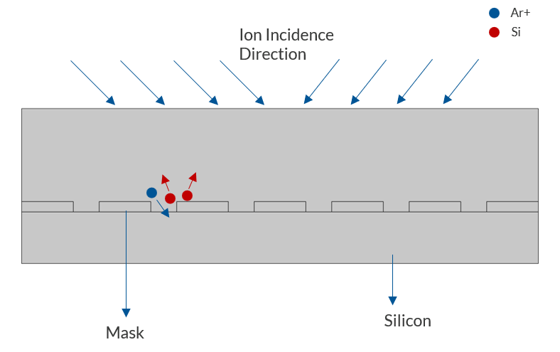 Representation of the model setup.
As seen in the image above, the sputtering process involves two ion beams incident at 45° and −45°, respectively. When argon ions hit the silicon surface, silicon atoms are sputtered. Each particle is assumed to represent 1012 actual argon ions. The mask height is taken as 0.2 μm, and the etching window width is 0.5 μm. Mask sputtering is ignored in this simplified example.
What the Results Depict
The figure below shows the sputtering yield in relation to the incident angle of the beam. Sputtering yield refers to the number of target atoms sputtered per incident ion. As can be seen, the number of secondary particles varies with respect to the angle of incidence. In this simplified model, the direction of secondary particle emission is assumed to follow a cosine distribution, and elastic-collision-based assumptions are used to estimate the emitted particle velocity. As observed in the graph, sputtering yield increases almost linearly with respect to incident angle between 30° and 70°. Accordingly, the sputtering yield can be calibrated by controlling the incident angle of the beam. For example, a lower angle of incidence can be employed for lesser material removal, whereas increasing the angle of the incident beam will result in more removal of target material within this range.
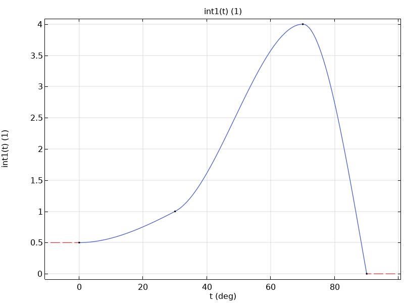 Number of secondary sputter particles with respect to the incident angle.
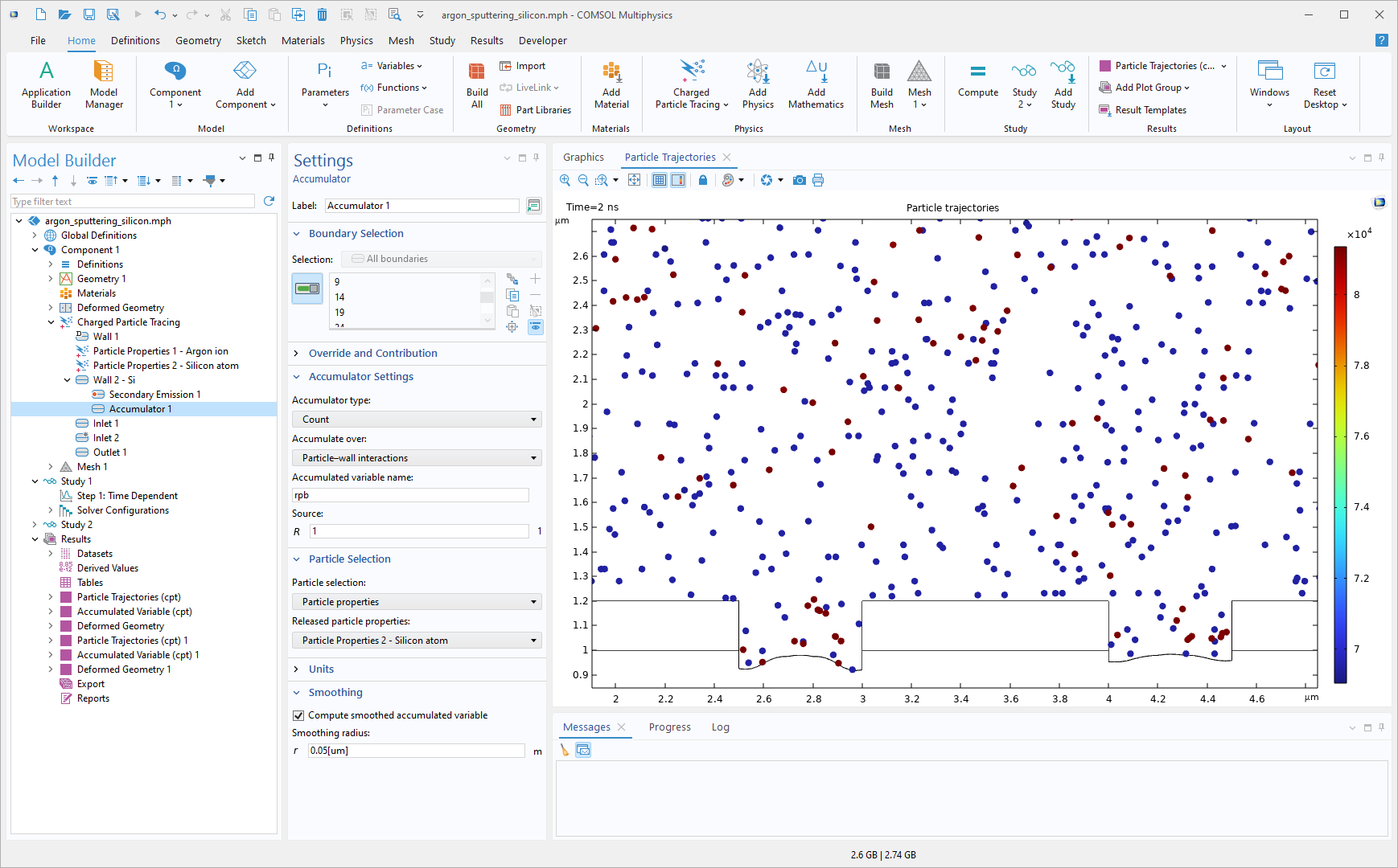 Particle trajectories and sputtering progression with beams incident at 45° and −45°.
The above figure depicts particle trajectories with beams incident at 45° and −45° and the resulting sputtering progression. More material is observed to be sputtered at the corners, resulting in faster height reduction.
How Can These Findings Be Improved?
This model can be further extended to incorporate other factors that affect sputtering. For example, in addition to the incident angle, sputtering yield also depends on the energy of the incident ion as well as the absolute and relative mass of the incident ion with respect to the target atoms. Furthermore, the bombardment process is significantly more complex in the real world, with some ions penetrating the substrate to generate cascading collisions and atoms being ejected only after multiple scattering events. These effects are not captured in this simplified model and generally require more specialized sputtering or collision-cascade descriptions.
Try It Yourself
Want to try modeling the sputtering process yourself? Download the related MPH-file in the Application Gallery:


Comments (0)