

Electromagnetic waves that are confined to propagate along a surface, such as surface plasmon polaritons (SPPs), are of great research interest due to their potential applications in nanoscale manipulation of light. In this blog post, we will discuss how to set up a simulation to visualize the propagation as well as the frequency-propagation constant dispersion relationship of SPPs.
Introduction to SPPs
The governing equations of electromagnetism, namely Maxwell’s equations, may seem simple, but their implications are extremely broad and profound. Therefore, propagating electromagnetic waves can exist in a variety of well-known forms — such as plane waves, spherical waves, Gaussian beams — and lesser-known forms — including Bessel beams, Airy beams, and vortex beams. There are also propagating electromagnetic waves that are confined in space, such as waveguide modes propagating in metallic or dielectric waveguides.
In addition, there is another special type of electromagnetic wave that is confined to a planar surface. This type of wave propagates tangentially to the surface and decays exponentially in the perpendicular direction. Its wavelength is often smaller when compared to the free space wavelength at the same frequency. Thus, this type of wave provides a potential technological platform for nanoscale control and manipulation of photons, which is desirable in many applications, ranging from optical communication and information processing to solar energy harvesting and digital display. The existence of this wave type was found on a metal-dielectric interface and is now known as surface plasmon polariton (SPP). (Plasmon refers to the collective oscillation of charges in the metal.) Since its discovery, it has been learned that many material systems support this type of surface wave, such as polar dielectric material near its phonon resonance frequencies and semiconductor material near its exciton frequency. The corresponding surface waves are named surface phonon polariton and surface exciton polariton, respectively.
Regardless of the supporting medium and the microscopic details, the macroscopic physics behind the different types of surface waves is similar. In the following sections, we will focus on modeling SPP between dielectric and metallic interfaces. However, it is important to note that the modeling techniques covered in this blog post can also be applied to other surface waves such as the Sommerfeld-Zenneck wave and Dyakonov wave in an analogous fashion with some suitable modifications.
Derivation of the Simplest SPP Dispersion
To develop a clear picture of what SPPs are, let’s investigate the simplest system that supports it, namely the bulk metal-dielectric interface. Imagine a metal-dielectric interface in the xz plane at y=0. The dielectric region is y>0 and the metal region is y<0. Since there is no preferred direction in the xz plane, without loss of generality, we focus on a surface wave that propagates in the x direction. The plane of propagation is defined as the plane spanned by the propagation direction and the surface normal. In this case, the plane of propagation is simply the xy plane. Generally, propagating electromagnetic waves can be categorized into s- or p-polarization, depending on whether the electric or magnetic field is perpendicular to the plane of propagation. Let’s first consider the p-polarization (or TM wave) case.
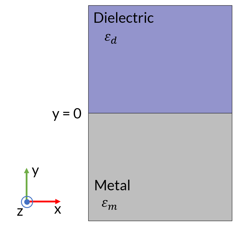
A metal-dielectric interface at y=0. This system supports SPPs that propagates in the x direction and exponentially decays in the y direction.
Since we are interested in a TM mode surface wave that propagates in the x direction and decays in the y direction, we can write the electric and magnetic fields in the dielectric and metal as
(1)
(2)
(3)
(4)
where the + and – superscripts denote quantities in y>0 and y<0, respectively. k_{SPP} is the complex SPP propagation constant. Both k_y^+ and k_y^- are positive real numbers that describe the decay of the field away from the metal-dielectric interface. Based on the boundary conditions, we know that the tangential components of the electric and magnetic fields, and the perpendicular component of the electric displacement field, are continuous across the metal-dielectric boundary at y=0. Therefore, E_x^+=E_x^-=E_x, H_z^+=H_z^-=H_z, and \varepsilon_dE_y^+=\varepsilon_mE_y^-=D_y. From Maxwell’s equations, we know that \nabla \cdot \vec{D} = \rho_{ext}. Since there is not external charge and the permittivity is constant in y>0 and y<0 separately, \nabla \cdot \vec{E} = 0 must hold in the two regimes. Combining this with Eqs. 2 and 4, we have
(5)
(6)
This simplifies to
(7)
From this relation, we can see why SPP only exists between a dielectric, Re(\varepsilon)>0, and a metal, Re(\varepsilon)<0. To have the field decay in the y direction, both k_y^+ and k_y^- must be positive, which means \varepsilon_d and \varepsilon_m must have opposite signs. To derive the expression for k_{SPP}, we use the Helmholtz wave equation \nabla^2 \vec{E}-\frac{\varepsilon \mu}{c^2} \frac{\partial^2E}{\partial t^2}=0, which is derived from the two Maxwell’s curl equations. Plugging Eqs. 2 and 4 into the Helmholtz equation leads to
(8)
(9)
where k_0=\omega/c is the free space wave number. Finally, combining Eqs. 7–9, we arrive at the expression for the SPP propagation constant
(10)
The real part of k_{SPP} is related to the SPP wavelength by \lambda_{SPP}=\frac{2\pi}{Re(k_{SPP})}, while the imaginary part describes the SPP propagation loss. Generally, \varepsilon_d and \varepsilon_m are frequency-dependent, so k_{SPP} is also frequency-dependent. The relationship of k_{SPP} and the frequency is often what we want to know to characterize the SPPs in a system.
Remember that the above discussion is purely based on the assumption that the SPP is a TM wave. For the possibility of the TE wave, one can simply follow the same derivation steps and show that all the field amplitudes must be zero. This means that SPPs only exist as a TM wave, which is also a distinctive feature of SPPs.
Simulating the Propagation and Dispersion of SPPs
In this section, we discuss how the simulation and modeling capabilities of the COMSOL Multiphysics® software can be used to visualize the physical results from the derivation above. Since SPPs are spatially confined propagating waves, we can take inspiration from other waveguide modeling examples, such as the Dielectric Slab Waveguide tutorial model. As a validity check to make sure we set up our model correctly, we will simulate the SPP in the interface of silver (metal) and air (dielectric). Silver’s dielectric function is well described by a Drude model with a plasma frequency value of around 9.6 eV. For this model, we can conveniently use the silver material properties in the software’s built-in material library. A numeric port is imposed on the left and right boundaries of the model. The left port with excitation turned on will launch the SPP, while the right port with excitation turned off will absorb the SPP without reflection. To get the mode field on both ports, two Boundary Mode Analysis study steps and a Frequency Domain study step are added, respectively.

Two ports are imposed on the left and right boundaries, respectively, for the excitation and termination of the SPP. To get the mode field on the ports, two Boundary Mode Analysis study steps are added before a Frequency Domain study step.
After running the simulation, we can easily visualize SPP propagation. From left to right, the animations below show the SPP at 3.54 eV, 3.1 eV, and 2.07 eV photon energy. As expected, the field propagates in the x direction and decays in the y direction. The decay is faster on the metal side due to the strong absorption. Noticeably, the SPP wavelength (real part of k_{SPP}) and the propagation loss (imaginary part of k_{SPP}) vary significantly with photon energy, or frequency. To capture the quantitative relationship between the frequency and k_{SPP}, we plot them using the variable frequency as the y-axis and ewfd.beta_1 as the x-axis (shown by the circle markers in the animations below). ewfd.beta_1 is a complex quantity, but when plotting it, it only considers its real part by default. When studying SPPs, it is customary to define a figure of merit, often referred to as the Q factor, as the ratio of the real part and the imaginary part of k_{SPP}. When k_{SPP} has a smaller imaginary part (equivalently, a larger Q factor), the SPP can propagate a long distance relative to its wavelength before it decays off. A larger Q factor is usually desirable for practical applications, such as biosensors and optical switches. The Q factor can conveniently be plotted as the color expression of the dispersion curve. Here, we chose a brighter color to represent the higher Q factor and a darker color to represent the lower Q factor. In addition, one dashed line representing \omega=ck_0, often called light line, is added. The light line is the frequency-wave number dispersion relation of free space photons. Lastly, the analytical expression from Eq. 9 is plotted as a solid curve. As we can see from the animations, the simulated dispersion and the analytical expression show good agreement.
Simulated SPP propagations at 3.54 eV, 3.1 eV, and 2.07 eV photon energy. The arrows indicate electric field direction and strength.
The dispersion plot below is very representative of the SPP dispersion in noble metals. This plot is useful for gaining insight on the characteristics of SPPs. Most importantly, it shows that the dispersion curve of SPPs always lies on the right side of the light line. The implication of this is that the SPP wavelength is always smaller than that of the free space light. This is why SPPs can be used as a way to compress the wavelength of light to achieve higher field concentration. Furthermore, the mismatch between free-space-light wave number and SPP propagation constant means that we cannot excite SPPs simply by shining light onto the metal surface, some external mechanism for the wave vector matching is required. The excitation of SPPs is often done by using total internal reflection from a prism, diffraction from a grating, scattering of a scatterer, or passing through an electron beam. The goal of using these techniques is to prepare the electromagnetic field so that its wave vector matches that of the SPP at the same frequency.
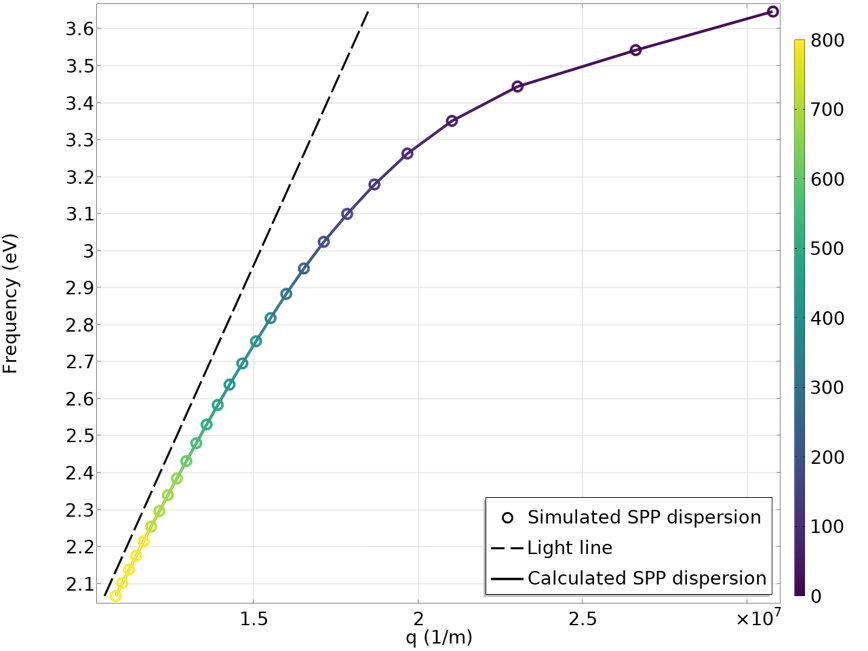
A plot of the simulated frequency-propagation constant dispersion of the SPP at the interface of silver and air. As expected, the simulated result (circles) is consistent with the analytical calculation (solid line). The free space light dispersion, or light line, is represented by a dashed line. The color represents the Q factor of SPP.
SPPs in Metal Thin Films
Although simulating SPPs in the bulk metal-dielectric interface serves as a helpful introduction to SPP propagation and dispersion, it is a rather simple and physically uninteresting example. In this section, we will cover a more interesting case of a metal thin film covered by dielectric layers. In this kind of system, both the top and bottom surfaces support SPPs. If the metal film is sufficiently thin, the coupling between the SPP on the top surface and the SPP on the bottom surface will lead to mode hybridization. The result of this is the formation of symmetric and antisymmetric modes. The physics in this situation is analogous to that of a coupled mechanical harmonic oscillators. In this particular case, we model a 12 nm aluminum film surrounded by 4 nm dielectric layers with a refractive index of 2. Using the Boundary Mode Analysis study step, we found two SPP branches in the dispersion curve. The upper branch with a larger Q factor is the symmetric mode, while the lower branch with a smaller Q factor is the antisymmetric mode.
Simulated SPP propagations on an aluminum thin film that is in-between two dielectric films. The hybridization of the SPPs in the top and bottom surfaces of the aluminum film form symmetric (left) and antisymmetric (right) modes.
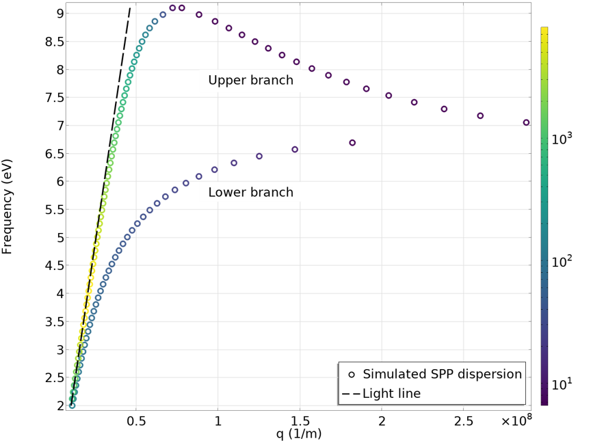
Simulated dispersion of the SPP on an aluminum thin film, sandwiched between two dielectric films. The symmetric (upper branch) and antisymmetric (lower branch) modes show up as two branches.
Although we don’t show it here, we can derivate the SPP dispersion in this kind of system analytically by carefully matching the boundary conditions at each interface. The derivation quickly becomes cumbersome as the geometry of the system gets more complex. The advantage of using COMSOL® for simulating SPPs lies in its flexibility, SPP dispersion can be computed in the software no matter how complex its geometrical composition is.
SPPs in Novel 2D Materials
2D materials are gaining tremendous popularity as the electronics industry is moving towards miniaturization. In our previous blog post, we introduced how to model a type of 2D material (graphene) in high-frequency electromagnetics. It turns out that 2D materials, such as graphene, can also support SPPs. After all, graphene with high conductivity behaves like metals. The main difference is that noble metals usually have a plasma frequency in the visible or ultraviolet regime, which means that metals support SPPs in the optical frequency. Graphene, on the other hand, supports SPPs in the infrared regime, making it a unique and advantageous material for certain applications, such as infrared harvesting and metamaterials. Another attractive property of graphene is that its conductivity can be changed by chemical doping or electric tuning. This opens up the tunability of SPPs, which is not achievable in conventional metals.
With the Simulating SPP Propagation and Dispersion tutorial model, we can investigate the SPPs in graphene deposited on an SiO2 substrate. The plots below show the dispersion curves with the graphene Fermi energy set to 0.2 eV (left) and 0.5 eV (right). A clear difference can be observed due to the difference in graphene conductivity. Compared to the SPP dispersion in metals, we can see that the light line here is very steep — it almost aligns with the y-axis. This is because the SPP propagation constant is much larger than the free-space-photon wave number. In other words, the SPP wavelength is much smaller. In the animation below, we can see the SPP propagation at 29 THz for the 0.2 eV Fermi energy case. At 29 THz, the free space wavelength is about 10 \mu m, while the SPP wavelength is less than 100 nm. A marvelous wavelength compression is achieved! However, we do need to note that the Q factor, in this case, is not very high. The SPP completely decays away after propagating only a few hundred nanometers. A higher Q factor can be achieved by improving the crystalline quality of graphene or cooling it down to cryogenic temperatures.


Dispersion curves for graphene SPPs with Fermi energy of 0.2 eV (left) and 0.5 eV (right).
Propagation of graphene SPP at 29 THz. The Fermi energy of graphene is set to 0.2 eV.
At first glance, it might seem strange that there is no SPP in a frequency range around 33 THz in the dispersion plots. This is due to the permittivity of the substrate material, SiO2, which turns negative as a result of its phonon resonance. This scenario can be seen by plotting the real part of the SiO2 permittivity in the simulation frequency range.
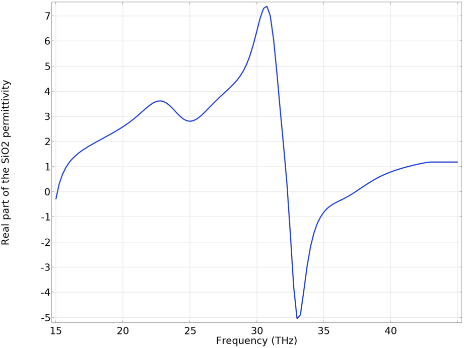
Real part of the SiO2 permittivity in the infrared frequency. Due to the phonon resonance, the permittivity becomes negative at around 33 THz, where the graphene SPP is not supported.
Earlier in this blog post, we briefly mentioned different experimental techniques that can be used to excite SPPs. Simulation offers alternative ways to excite SPP. One example is to use an electric point dipole source. Recall that SPP cannot be excited by free space light due to the wave vector mismatch. However, the near field created by the point dipole contains components with large wave vectors, which allows for SPP to be excited. One can also map out the SPP dispersion by performing such a simulation and extracting the SPP wavelength from the field distribution. This type of simulation is highlighted in the figure below, where clear field oscillations can be observed.
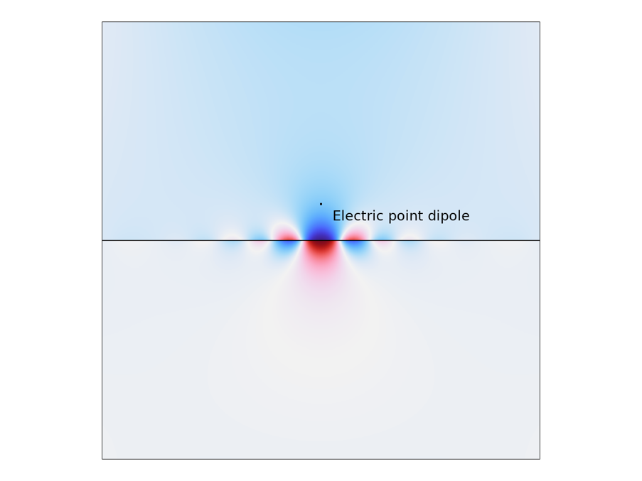
Graphene SPP excited by an electric point dipole oriented in the y direction.
Concluding Remarks
As mentioned, SPPs are only one of the many special classes of surface waves. Electromagnetic surface waves are still undergoing intensive research and their observable phenomena goes beyond the scope of this blog post. For example, some anisotropic materials, such as MoO3, can support unidirectional surface phonon polariton. This is because at a certain frequency, only the permittivity in one in-plane direction is negative. In the animation below, we can see such a case where an MoO3 slab on an SiO2 substrate is excited by an electrical point dipole. The surface phonon polariton propagates in a “butterfly” pattern that is distinctive to the SPP in, for example, graphene, where the launched SPP propagates isotopically.
Anisotropic surface phonon polariton propagation in MoO3 slab excited by an electric point dipole.
By utilizing the features in COMSOL Multiphysics®, such as the Electric Point Dipole node and the Boundary Mode Analysis study, one can model electromagnetic surface waves in many different ways and explore the associated rich phenomena.
Next Step
- Further explore the models discussed in this blog post in the Application Gallery, where they are available for download:
- In addition to the examples above, you can find many other surface plasmon polariton example models in the Application Gallery, including:
Reference
- S. A. Maier, Plasmonics: fundamentals and applications. Springer, 2007.


Comments (6)
Noah Bright
April 21, 2023Hi Xinzhong,
Really good introduction to SPPs. Covers all the fundamentals and then some.
I’d like to run some simulations like your last few, coupling dipole radiation to SPPs. Are there any example simulations like that? The two that are linked don’t seem to cover that part.
Noah
Zhu Juanfeng
June 1, 2023Hi XinZhong,
Thanks for your introduction to stimulate the SPP. May you tell me that how to simulate the field distribution in anisotropic materials ( for example, MoO3)? There were many reflections in my simulation model, and I am confoused that how to elimiate the reflection,
Lokesh Ahlawat
March 30, 2024Hi, Zhu Juanfeng
Did you get to know the mentioned problem?
Sergey Yankin
December 3, 2024 COMSOL EmployeeHello!
The best way to sort out the reason you get unexpected reflections is to submit a support case so that our team can check your model and get the bearing about the reason for it: https://www.comsol.com/support
Best regards
Sergey Yankin
COMSOL Technical Support
Sergey Yankin
December 3, 2024 COMSOL EmployeeHello!
The best way to sort out the reason you get unexpected reflections is to submit a support case so that our team can check your model and get the bearing about the reason for it: https://www.comsol.com/support
Best regards
Sergey Yankin
COMSOL Technical Support
Patrik Micek
February 14, 2026Hi, could you please explain how to plot the symmetric & anti-symmetric Ey field profiles from the “SPPs in Metal Thin Films” section? Using the study1 and changing the wavelength still gives the anti-symmetric mode, without the option to choose the effective index of the mode.
Thanks for the answer,
Patrik