
Besi Improved Memory Chip Manufacturing with Multiphysics Simulation
Stefan Behler, Besi, Switzerland
As memory chips become smaller and smaller, designers must ensure that the chips stay intact during the manufacturing process. Besi develops equipment and assembly processes for substrate and wafer packaging production in markets such as consumer electronics, automotive, industrial, and solar energy. Stefan Behler, a senior expert process engineer, used multiphysics simulation to explore and optimize a new way of peeling off the tape on a memory chip that results in less deformation of the dies. This new method is now used by semiconductor packaging factories all over the world.
Suggested Stories
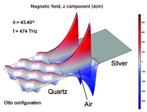
Surface Plasmon Resonance
Surface Plasmon Resonance (SPR) is created by surface plasmons, coherent electron oscillations existing between any ...

Fine Tuning for Water Purification
Amsterdam Water Supply (AWS) of the Netherlands produces some of the cleanest drinking water in the world using an ...
Democratizing Simulation with Applications
Veryst Engineering, AltaSim Technologies, and GLL Bio-Med Analytics build applications in COMSOL Multiphysics ...
Keynote: The Role of FEA Simulations in Electrifying Aviation
In this keynote talk, Mustafa Baris Topçuoglu discusses aerospace company GKN Fokker Elmo's research- and customer ...


