
Besi Improved Memory Chip Manufacturing with Multiphysics Simulation
Stefan Behler, Besi, Switzerland
As memory chips become smaller and smaller, designers must ensure that the chips stay intact during the manufacturing process. Besi develops equipment and assembly processes for substrate and wafer packaging production in markets such as consumer electronics, automotive, industrial, and solar energy. Stefan Behler, a senior expert process engineer, used multiphysics simulation to explore and optimize a new way of peeling off the tape on a memory chip that results in less deformation of the dies. This new method is now used by semiconductor packaging factories all over the world.
Suggested Stories
Graphene Paves the Way for Next-Generation Plasmonics
Alexander V. Kildishev, associate professor of electrical and computer engineering, is leading computational ...
Get a Quick Look at How Plastometrex Uses COMSOL Compiler™
Step into the world of the startup company Plastometrex to see how they developed an efficient method for measuring ...
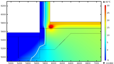
Using Multiphysics Simulation to Prevent Building Damage
In addition to surviving normal winters, a strong building must be able to survive the worst winters expected in a 50 ...
Keynote: Simulation of MEMS Sensors at Bosch
In this keynote talk at the COMSOL Conference 2025 Amsterdam, Daniel Maier of Bosch discusses MEMS sensors and the ...


