
Besi Improved Memory Chip Manufacturing with Multiphysics Simulation
Stefan Behler, Besi, Switzerland
As memory chips become smaller and smaller, designers must ensure that the chips stay intact during the manufacturing process. Besi develops equipment and assembly processes for substrate and wafer packaging production in markets such as consumer electronics, automotive, industrial, and solar energy. Stefan Behler, a senior expert process engineer, used multiphysics simulation to explore and optimize a new way of peeling off the tape on a memory chip that results in less deformation of the dies. This new method is now used by semiconductor packaging factories all over the world.
Suggested Stories
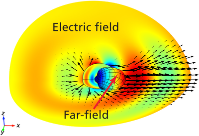
Scattering of Electromagnetic Waves by Particles
When electromagnetic waves propagate through matter, they interact with inhomogeneities and particles that can locally ...

Analysis of Subsea Umbilicals and Cables
JDR Cables designs-to-spec and manufactures subsea umbilical systems of cables and reelers for the oil and gas and ...
Modeling of Complex Physics Speeds Chip Development
With technological advancements accelerating so rapidly, more powerful computer chips are needed to meet the high ...
Innovative Motor Designs for Electric Cars Come to Life
If electric vehicles are to ultimately transcend from niche to mainstream, their motor designs must continually ...


