
Besi Improved Memory Chip Manufacturing with Multiphysics Simulation
Stefan Behler, Besi, Switzerland
As memory chips become smaller and smaller, designers must ensure that the chips stay intact during the manufacturing process. Besi develops equipment and assembly processes for substrate and wafer packaging production in markets such as consumer electronics, automotive, industrial, and solar energy. Stefan Behler, a senior expert process engineer, used multiphysics simulation to explore and optimize a new way of peeling off the tape on a memory chip that results in less deformation of the dies. This new method is now used by semiconductor packaging factories all over the world.
Suggested Stories
It’s a Bird, It’s a Plane: Flow Patterns around an Oscillating Piezoelectric Fan Blade
As electronics grow smaller and smaller and are used for extensive periods of time, their internal heat loads are ...
Restoration of Lake Water Environments
Human activity steals oxygen from natural water sources such as lakes and this oxygen-deficient water often contains ...
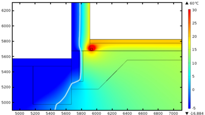
Using Multiphysics Simulation to Prevent Building Damage
In addition to surviving normal winters, a strong building must be able to survive the worst winters expected in a 50 ...
Peeling Away Memory Chips
As memory chips become smaller and smaller, designers must ensure that the chips stay intact during the manufacturing ...


