
Besi Improved Memory Chip Manufacturing with Multiphysics Simulation
Stefan Behler, Besi, Switzerland
As memory chips become smaller and smaller, designers must ensure that the chips stay intact during the manufacturing process. Besi develops equipment and assembly processes for substrate and wafer packaging production in markets such as consumer electronics, automotive, industrial, and solar energy. Stefan Behler, a senior expert process engineer, used multiphysics simulation to explore and optimize a new way of peeling off the tape on a memory chip that results in less deformation of the dies. This new method is now used by semiconductor packaging factories all over the world.
Suggested Stories
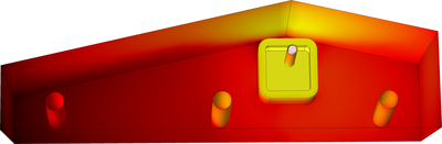
Continuous Casting: Optimizing Both Machine and Process with Simulation
The process of continuous casting has transformed steel production, saving valuable resources while improving steel ...
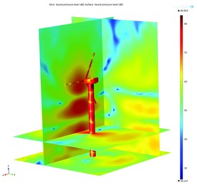
Wind Turbine Noise Reduction
Xi Engineering Consultants Ltd specializes in complex vibration issues, like those caused by wind turbines. The ...
Multiphysics Analysis Advances Water Main Leak Detection
As infrastructure ages and becomes obsolete, municipalities must deal with the constant updating and renovating ...
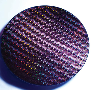
Pushing the Limits of Chip Density
Chip manufacturers have been adhering to Moore’s law, a law stating that the number of transistors that can be ...


