
Besi Improved Memory Chip Manufacturing with Multiphysics Simulation
Stefan Behler, Besi, Switzerland
As memory chips become smaller and smaller, designers must ensure that the chips stay intact during the manufacturing process. Besi develops equipment and assembly processes for substrate and wafer packaging production in markets such as consumer electronics, automotive, industrial, and solar energy. Stefan Behler, a senior expert process engineer, used multiphysics simulation to explore and optimize a new way of peeling off the tape on a memory chip that results in less deformation of the dies. This new method is now used by semiconductor packaging factories all over the world.
Suggested Stories
Behind the Rumble and Roar of Mahindra Motorcycles
Optimization is a subtle and delicate art, especially when it comes to motorcycles. Regulatory requirements on pass-by ...
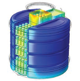
Innovative Thermal Insulation Techniques Bring Vaccines to the Developing World
When medical professionals transport vaccines, their cargo needs to be kept at a cool temperature. This limits their ...
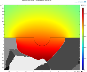
Simulation-Led Strategy for Corrosion Prevention
Corrosion is a widespread concern costing the US billions of dollars annually. For the Navy, specifically, it is the ...
From Nanoantennas to Deep Space Satellites, Electron Emission Enables Efficient Power Generation
Researchers from the Italian Institute of Technology (IIT) and the European Space Agency (ESA) are developing power ...


