
Besi Improved Memory Chip Manufacturing with Multiphysics Simulation
Stefan Behler, Besi, Switzerland
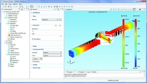
As memory chips become smaller and smaller, designers must ensure that the chips stay intact during the manufacturing process. Besi develops equipment and assembly processes for substrate and wafer packaging production in markets such as consumer electronics, automotive, industrial, and solar energy. Stefan Behler, a senior expert process engineer, used multiphysics simulation to explore and optimize a new way of peeling off the tape on a memory chip that results in less deformation of the dies. This new method is now used by semiconductor packaging factories all over the world.
Suggested Stories
3D Parametric Full Eye Model Gives 20+ Years of Better Vision
To correct presbyopia, researchers at Kejako, a medical device company in Switzerland, are developing a noninvasive ...
Optimization Slashes Energy Consumption in Silicon-Based MEMS CO2 Detectors
CEA-MINATEC is an international center for micro and nano-technologies which is funded by CEA, a French government ...
Designing an Eco-Friendly Anode Baking Process with Numerical Modeling
Aluminum is extracted through the Hall–Héroult process, during which it is removed from bauxite using green anodes. A ...
Multiphysics Analysis Advances Water Main Leak Detection
As infrastructure ages and becomes obsolete, municipalities must deal with the constant updating and renovating ...


