Simulation of Sample Inhomogeneity in Microwave Impedance Microscopy
Microwave impedance microscopy (MIM) is a novel mode of atomic force microscopy that can measure topography and local electrical impedance simultaneously and with nanometer spatial resolution [1]. This technique is typically used qualitatively, identifying defects in nanodevices or imaging ferroelectric domain walls, for example. However, the technique also has the potential to be used in a more rigorous analysis of materials, possibly identifying systematically how specific structural features can give rise to variations in electrical properties. We have chosen to study different porous carbon materials for their diverse structure and electrical properties, and interesting applications, especially in energy storage. In order to elucidate any correlation between structure and electrical behavior in these samples, facilitating the interpretation of MIM results, various models of the probe-sample system have been simulated via finite element analysis in COMSOL Multiphysics® software.
The MIM instrument consists of a 3 GHz electrical source coupled to an AFM tip, sketched in Figure 1. As the tip scans across the surface of a sample, both the sample topography and the amount of reflection of electrical signal (S11) are recorded. The instrument is designed to measure the interaction between the sample and evanescent wave modes emanating from the tip. Since evanescent waves decay exponentially in amplitude with increasing distance away from the tip, the volume of non-negligible interaction has a characteristic spatial dimension much less than the free-space wavelength at 3 GHz (10 cm). Thus, it is sufficient to model the electrical phenomena in the system using a quasistatic approximation of Maxwell's equations, as implemented using the COMSOL AC/DC Module. The MIM electronics report the change in impedance between the tip and sample at each point in the AFM scan, and because COMSOL software can easily compute electrical impedance between any pair of specified terminals, the simulation results are closely related to the data collected in a real measurement.
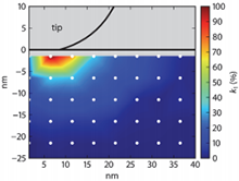
The porous carbon materials studied in MIM experiments thus far include carbide-derived carbon [2], nanodiamond, and onion-like carbon [3]. These materials can exhibit a broad range of structures and electrical properties based on synthesis conditions. They also have disordered structures with nanoscopic variation in features that typically have a strong influence over their performance in applications. As such, they represent interesting systems of study for MIM. However, their inhomogenous structure poses a challenge to modeling efforts. We have chosen first to simulate a homogeneous sample, develop an equivalent circuit as shown in Figure 2, then add additional domains in the sample of different material properties than the host matrix to represent pores. The simple case of one inclusion, as in Figure 3 where the change in tip-sample conductance is mapped for different pore locations, shows the maximum size of the interrogated volume. The case of two inclusions, as in Figure 4, shows how the arrangement of pores may affect the electrical impedance and so the MIM signal strength.
Download
- jones_paper.pdf - 0.62MB
- jones_abstract.pdf - 0.45MB