
COMSOL Multiphysics Modeling of Self-Assembled Semiconductor Quantum Dots
Semiconductor quantum dots (QDs) play a critical role in next-generation optoelectronic devices, including high-efficiency lasers and light-emitting diodes (LEDs). This importance arises from the discrete energy levels of QDs and their tunable emission properties. For device engineers, there is a growing need for simulation tools that are accurate, accessible, and adaptable to realistic QD geometries and material compositions. However, integrating strain effects, heterostructure physics, and quantum confinement into a single practical modeling workflow remains a significant challenge.
In this work, we present a unified modeling framework implemented entirely within COMSOL Multiphysics® using the Mathematics Module and the Coefficient Form PDE interface. The model combines continuum elasticity with quantum mechanical band-structure calculations. Strain and piezoelectric effects are obtained by solving coupled partial differential equations for displacement, stress, and polarization fields. These fields directly modify the band-edge potential in QDs. The resulting outputs are seamlessly coupled into an eigenvalue problem describing carriers' bound states. The conduction band is treated using an effective mass model, while the valence band is described by a four-band k·p Hamiltonian that captures heavy-hole and light-hole band mixing. The finite element method (FEM) enables accurate treatment of realistic QD sizes, geometric shapes, and material compositions.
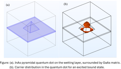
This framework enables simultaneous investigation of (1) strain effects in semiconductor QDs, (2) coupling between the wetting layer and the quantum dot, and (3) bound-state energies and wavefunctions. These capabilities are essential for understanding carrier confinement, leakage, and recombination processes. These processes directly impact the performances of optoelectronic devices, such as laser threshold current, emission wavelength, and LED efficiency. From an application perspective, the workflow is designed for rapid parametric studies and efficient design iteration. This makes it suitable for both academic research and industrial device development. Current models include III–V semiconductor compounds with QDs in pyramidal or lens-shaped geometries. Because the entire implementation resides within the COMSOL environment, the model is portable, reproducible, and easily extended to a wide range of QD material systems and geometries.
In conclusion, this work demonstrates a practical semiconductor QD simulator implemented in COMSOL. The proposed approach bridges the gap between simplified analytical models and computationally intensive atomistic methods. It offers engineers a powerful and flexible tool for the design and optimization of quantum dot materials.
Download
- COMSOL Poster 2026 Boston_WLI.pdf - 0.63MB


