
Besi Improved Memory Chip Manufacturing with Multiphysics Simulation
Stefan Behler, Besi, Switzerland
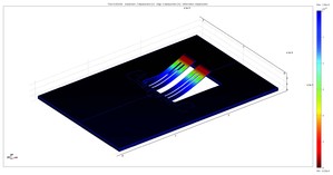
As memory chips become smaller and smaller, designers must ensure that the chips stay intact during the manufacturing process. Besi develops equipment and assembly processes for substrate and wafer packaging production in markets such as consumer electronics, automotive, industrial, and solar energy. Stefan Behler, a senior expert process engineer, used multiphysics simulation to explore and optimize a new way of peeling off the tape on a memory chip that results in less deformation of the dies. This new method is now used by semiconductor packaging factories all over the world.
Suggested Stories
Easy and Accurate Measurement of Blood Viscosity
Microvisk Technologies develops and manufactures devices for measuring blood viscosity using the power of Micro ...
Designing a Lightweight Hyperloop Pod with Composite Materials
The EPFLoop team competed at the 2019 SpaceX Hyperloop Pod Competition with a Hyperloop pod that was half the weight ...
Engineering Perfect Puffed Snacks
The production of puffed rice, like many other types of food, is incredibly complicated and involves multiple ...
Lightweighting with Aluminum: Corrosion Apps Guide Leading Design
To achieve fuel efficiency goals, conventional materials for car structures, such as structural steel, must be ...


