
Besi Improved Memory Chip Manufacturing with Multiphysics Simulation
Stefan Behler, Besi, Switzerland
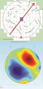
As memory chips become smaller and smaller, designers must ensure that the chips stay intact during the manufacturing process. Besi develops equipment and assembly processes for substrate and wafer packaging production in markets such as consumer electronics, automotive, industrial, and solar energy. Stefan Behler, a senior expert process engineer, used multiphysics simulation to explore and optimize a new way of peeling off the tape on a memory chip that results in less deformation of the dies. This new method is now used by semiconductor packaging factories all over the world.
Suggested Stories
Inspiring Young Engineers to Design for the Future at EPFL
EPFLoop, from the Swiss Federal Institute of Technology Lausanne (EPFL), designed their pod for the 2018 SpaceX ...
Modeling of Complex Physics Speeds Chip Development
With technological advancements accelerating so rapidly, more powerful computer chips are needed to meet the high ...
Getting Touchy-Feely with Touchscreen Design
We rely on capacitive touchscreens whenever we interact with a smartphone, MP3 device, or car video screen. ...
A STEP in the Right Direction: Modeling AC Losses in a Tokamak Design
The Spherical Tokamak for Energy Production (STEP) program aims to deliver a prototype fusion energy plant in the ...


