
Besi Improved Memory Chip Manufacturing with Multiphysics Simulation
Stefan Behler, Besi, Switzerland
As memory chips become smaller and smaller, designers must ensure that the chips stay intact during the manufacturing process. Besi develops equipment and assembly processes for substrate and wafer packaging production in markets such as consumer electronics, automotive, industrial, and solar energy. Stefan Behler, a senior expert process engineer, used multiphysics simulation to explore and optimize a new way of peeling off the tape on a memory chip that results in less deformation of the dies. This new method is now used by semiconductor packaging factories all over the world.
Suggested Stories
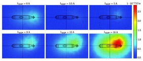
Submarines: Corrosion Protection or Enemy Detection?
Submarines create underwater electric potential (UEP) signatures when using corrosion protection systems. These ...
Democratizing Simulation with Applications
Veryst Engineering, AltaSim Technologies, and GLL Bio-Med Analytics build applications in COMSOL Multiphysics ...
Multiphysics Analysis Advances Water Main Leak Detection
As infrastructure ages and becomes obsolete, municipalities must deal with the constant updating and renovating ...
Simulation Applications Help Shape the Design of Car Audio Systems
Audio entertainment systems for luxury cars must provide end users with the highest quality of in-car listening ...


