Defying Convention to Achieve Faster Signal and Simulation Speeds
Juan C. Cervantes-Gonzalez, Intel Guadalajara Design Center, MexicoAs the demand grows for faster electronic devices in smaller packages, we need to develop optimized high-speed interconnects, which transfer the signal between components in electronic devices. Found in printed circuit boards (PCB), this integral design element in electronics packaging carries signals laterally and through the depth of PCBs, traversing many layers of metal and dielectric material. To satisfy these growing technology demands, interconnects must be designed smaller, more closely packed, and able to operate at higher frequencies.
To reduce the number of prototypes required to test new interconnect designs, engineers at the Intel Guadalajara Design Center developed an efficient computational design optimization method, combining full-wave electromagnetic simulation in COMSOL Multiphysics® software with a space-mapping (SM) algorithm implemented in MATLAB® software. Through their approach, an interconnect design can be quickly optimized, streamlining the design cycle and time to market of the latest high-speed interconnect technology.
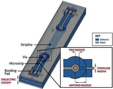 Model geometry of a single-ended interconnect set up in COMSOL Multiphysics® software.
Download
- Intel_MS2015.pdf - 0.42MB