
La Galleria delle Applicazioni raccoglie un'ampia varietà di tutorial e di app dimostrative realizzati con COMSOL Multiphysics in diversi ambiti applicativi, inclusi quelli elettrico, meccanico, fluidico e chimico. E' possibile scaricare i file dei modelli e delle app demo pronti all'uso e le istruzioni step-by-step per costruirli, e utilizzarli come punto di partenza per le proprie simulazioni.
Lo strumento di Ricerca Rapida permette di trovare i modelli che si riferiscono alla propria area di interesse.
Si noti che molti degli esempi qui presentati sono accessibili anche tramite le Librerie delle Applicazioni incorporate nel software COMSOL Multiphysics® e disponibili dal menu File.
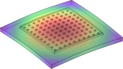
Flip chip (FC) is a widely used form of advanced semiconductor packaging that yields high interconnection density and good signal transmission performance of the semiconductor device as well as a reduction in size. In FC devices, the chip is placed face down and directly bonded to the ... Per saperne di più
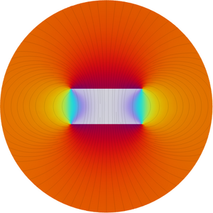
Permanent magnet manufacturers test magnets by applying a cyclic temperature load during the design process to assess the resulting thermal demagnetization. The heating process is usually slow enough that the temperature distribution inside the magnet can be considered uniform at any ... Per saperne di più
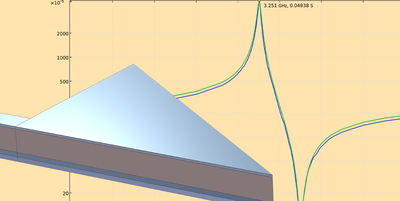
This model demonstrates how to extract the lumped parameters for an mBVD equivalent circuit from a FEM simulation and how to leverage such a model directly using the Electrical Circuit interface. A 3D layered FBAR resonator is considered as an example. Related Blog Post Leveraging the ... Per saperne di più
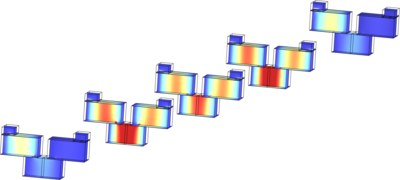
Cascaded cavity filters provide much better bandpass filter performance than single cavity filters. This example demonstrate how to use shape optimization to optimize three rectangular cavity filters coupled via slots. The calculated S-parameters show excellent out-of-band rejection. Per saperne di più
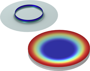
In direct bonding, the in-plane relative displacement between corresponding points on the bonding surfaces of the top and bottom wafers, denoted as IPD (In-Plane Distortion), is the primary yield killer in the bonding process. This model can predict the entire direct wafer bonding ... Per saperne di più
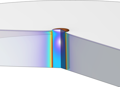
Through-silicon vias (TSVs) allow chips or wafers to be connected vertically, making TSV a crucial technology for 2.5D and 3D packaging. The basic structure of a TSV consists of a deep hole penetrating a silicon substrate, a filling metal (usually copper) in the deep hole, and an ... Per saperne di più
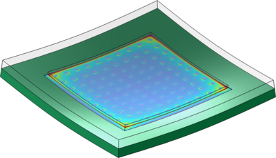
Flip-chip (FC) is one of the advanced forms of semiconductor device packaging that is widely used in today's semiconductor packages for its capability to minimize packaging size while enhancing electrical interconnection density and transmission performance. In FC devices, the active ... Per saperne di più
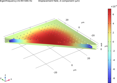
This tutorial demonstrates how to import a GDS file to model a capacitive micromachined ultrasonic transducer (CMUT). It shows how to define the layer stackup by modifying layer thicknesses and elevations, and how to use the automatically generated layer and cell selections. The imported ... Per saperne di più


